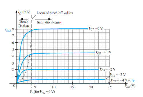
a. Determine VDS for VGS = 0 V and ID = 6 mA using the characteristics of Fig. 6.11b. Usin...
a. Determine VDS for VGS = 0 V and ID = 6 mA using the characteristics of Fig. 6.11
b. Using the results of part (a), calculate the resistance of the JFET for the region ID = 0 to 6 mA for VGS= 0V.
c. Determine VDS for VGS = −1V and ID = 3 mA.
d. Using the results of part (c), calculate the resistance of the JFET for the region ID = 0 to 3 mA for VGS = −1V.
e. Determine VDS for VGS = −2 V and ID = 1.5 mA.
f. Using the results of part (e), calculate the resistance of the JFET for the region ID = 0 to 1.5 mA for VGS = −2V.
g. Defining the result of part (b) as ro, determine the resistance for VGS = −1 V using Eq. (6.1) and compare with the results of part (d).
h. Defining the result of part (b) as ro, determine the resistance for VGS = −2 V using the same equation, and compare the results with part (f).
i. Based on the results of parts (g) and (h), does Eq. 6.1, appear to be a valid approximation?
FIG. 6.11 n-Channel JFET characteristics with IDSS = 8 mA and VP = -4 V.
 (6.1)
(6.1)
Step-by-Step Solution
Request Solution!
We need at least 8 more requests to produce the solution.
2 / 10 have requested this problem solution
The more requests, the faster the answer.
Most questions answered within 3 hours.
-
Calculating the space time for parallel reactions. m-Xylene is reacted over a ZSM-5 zeolit...
-
Determine Vo and ID for the networks of Fig. 2.160.FIG. 2.160
-
The truck travels along a circular road that has a radius of 50 m at a speed of 4 m/s. F...
-
A state legislature enacted a statute that required any motorcycle operator or passenger...
-
A 1024 × 1024 8-bit image with 5.3 bits/pixel entropy [computed from its histogram using E...
-
In Problem 3.3, we estimated the equationwhere we now report standard errors along with th...
-
In each of the following cases, deduce the nature of the light that is consistent with the...
-
Solve Example 20.5 such that the x, y, z axes move with curvilinear translation, Ω = 0 in...
-
In Fig. 6.43, if i = cos 4t and v = sin 4t, the element is:(a)a resistor(b) a capacitor(c)...
-
Sketch vo for each network of Fig. 2.181 for the input shown.FIG. 2.181
-
(Supplement B) Computing and Reporting Cash Flow Effectsof Sale of Plant and EquipmentDuri...
-
A 350-mL spherical flask contains 0.075 mol of an ideal gas at a temperature of 293 K. Wha...