
Homework Answers
Add Answer to:
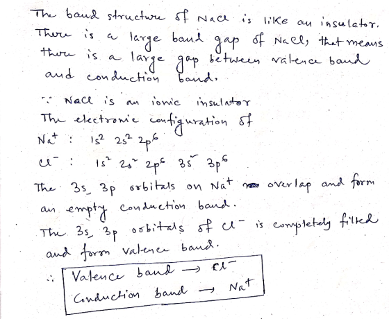
1. What is the band structure of NaCl? What atoms make up the valence band and...
Band structure Consider a one-dimensional semiconductor crystal consisting of 11 atoms with nearest- neighbor atoms separated...
 Band structure Consider a one-dimensional semiconductor crystal consisting of 11 atoms with nearest- neighbor atoms separated by a 5 . The band structure for electrons in the conduction band is given by Ec(k) = 101(k-0.2n)2-A(k-02n)"] + 2.25 [eV] and the band structure for holes in the valence band is given by where the wavevector k s in units ofA-1. The allowed wavevectors are--< k 즈 al (a) Is this a direct or indirect gap semiconductor? What is the energy gap...
(Optional, 12 bonus points) Consider a imensional semiconductor with a band structure as shown in...
 (Optional, 12 bonus points) Consider a imensional semiconductor with a band structure as shown in the diagram. The dispersion relations of the conduction and valence bands are given as: Ew.c where Ew.c>Ew, i) What is the band gap of this ii) Please find the electron effective mass at iii) Please find the hole effective masses at the iv) It is known that Ew,v
Conduction band Energy gap, Valence band The energy gap between the valence band and the conduction...
 Conduction band Energy gap, Valence band The energy gap between the valence band and the conduction band in the widely-used semiconductor gallium arsenide (GaAs) is A - 1.424 eV. Suppose that we consider a small piece of GaAs with 1020 available electrons, and use the equilibrium condition derived in the prelecture. 1) On average, how many electrons will be in the conduction band if T-282.15 K? electrons Submit 2) How many holes (the white dots in the figure) will be...
If an element has a band gap of 1 eV between a filled valence band and...
If an element has a band gap of 1 eV between a filled valence band and an empty conduction band, it would be classified as a?
(A) Comment on the energy needed to excite an electron from the valence band edge to...
 (A) Comment on the energy needed to excite an electron from the valence band edge to conduction band edge of InP if the temperature is reduced from 300K to 77K. Justify your answer (B) If the semiconductor is undoped, how does the probability of occupancy of a state at the conduction band edge change as the temperature of the semiconductor is increased? Justify your answer.
The energy gap between the valence band and the conduction band in the widely-usd semiconductor gallium...
 The energy gap between the valence band and the conduction band in the widely-usd semiconductor gallium arsenide (GaAs) is A- 1.424 ev. (k 8.617x10⁵ eV/K) At T 0 K the valence band has all the electrons. At T 0 K (shown), electrons are thermally excited across the gap into the conduction band, leaving an equal number of holes behind. Conduction band Energy gap, A Valence band 1) The density of free electrons (ne number per volumer) in a pure crystal...
Please help me 1. In degenerate p-type silicon, a. The Fermi energy is above the valence...
 Please help me
1. In degenerate p-type silicon, a. The Fermi energy is above the valence energy and below the intrinsic Fermi energy b. The Fermi energy is below the valence energy c. The Fermi energy is above the conduction energy d. The Fermi energy is below the conduction energy and above the intrinsic Fermi energy 2. A semiconductor has No 5X 1010 cm3 and N-2X 1018 cm2. It is a. b. C. d. N-type and electrons are the majority...
Please help me
1. In degenerate p-type silicon, a. The Fermi energy is above the valence energy and below the intrinsic Fermi energy b. The Fermi energy is below the valence energy c. The Fermi energy is above the conduction energy d. The Fermi energy is below the conduction energy and above the intrinsic Fermi energy 2. A semiconductor has No 5X 1010 cm3 and N-2X 1018 cm2. It is a. b. C. d. N-type and electrons are the majority...
(1) What is the valence electron configuration for the arsenic atom? (2) What is the valence...
(1) What is the valence electron configuration for the arsenic atom? (2) What is the valence electron configuration for the calcium atom? (1) What is the name of the element with a valence electron configuration of 2s22p2? (2) What is the name of the element with a valence electron configuration of 4s24p1?
4. A photon of light can excite an electron from the valence band to the conduction...
 4. A photon of light can excite an electron from the valence band to the conduction band of a semiconductor. This process is called photoconduction. a. PbS has a band gap of 0.37 eV. What wavelength of light would be needed to start the photoconduction in this semiconductor? b. In the light meters of cameras one would need a semiconductor that operates efficiently in visible light, or at-550 nm. Would PbS be a suitable semiconductor for a light meter? Why...
 Band structure Consider a one-dimensional semiconductor crystal consisting of 11 atoms with nearest- neighbor atoms separated by a 5 . The band structure for electrons in the conduction band is given by Ec(k) = 101(k-0.2n)2-A(k-02n)"] + 2.25 [eV] and the band structure for holes in the valence band is given by where the wavevector k s in units ofA-1. The allowed wavevectors are--< k 즈 al (a) Is this a direct or indirect gap semiconductor? What is the energy gap...
 (Optional, 12 bonus points) Consider a imensional semiconductor with a band structure as shown in the diagram. The dispersion relations of the conduction and valence bands are given as: Ew.c where Ew.c>Ew, i) What is the band gap of this ii) Please find the electron effective mass at iii) Please find the hole effective masses at the iv) It is known that Ew,v
 Conduction band Energy gap, Valence band The energy gap between the valence band and the conduction band in the widely-used semiconductor gallium arsenide (GaAs) is A - 1.424 eV. Suppose that we consider a small piece of GaAs with 1020 available electrons, and use the equilibrium condition derived in the prelecture. 1) On average, how many electrons will be in the conduction band if T-282.15 K? electrons Submit 2) How many holes (the white dots in the figure) will be...
 (A) Comment on the energy needed to excite an electron from the valence band edge to conduction band edge of InP if the temperature is reduced from 300K to 77K. Justify your answer (B) If the semiconductor is undoped, how does the probability of occupancy of a state at the conduction band edge change as the temperature of the semiconductor is increased? Justify your answer.
 The energy gap between the valence band and the conduction band in the widely-usd semiconductor gallium arsenide (GaAs) is A- 1.424 ev. (k 8.617x10⁵ eV/K) At T 0 K the valence band has all the electrons. At T 0 K (shown), electrons are thermally excited across the gap into the conduction band, leaving an equal number of holes behind. Conduction band Energy gap, A Valence band 1) The density of free electrons (ne number per volumer) in a pure crystal...
 Please help me
1. In degenerate p-type silicon, a. The Fermi energy is above the valence energy and below the intrinsic Fermi energy b. The Fermi energy is below the valence energy c. The Fermi energy is above the conduction energy d. The Fermi energy is below the conduction energy and above the intrinsic Fermi energy 2. A semiconductor has No 5X 1010 cm3 and N-2X 1018 cm2. It is a. b. C. d. N-type and electrons are the majority...
Please help me
1. In degenerate p-type silicon, a. The Fermi energy is above the valence energy and below the intrinsic Fermi energy b. The Fermi energy is below the valence energy c. The Fermi energy is above the conduction energy d. The Fermi energy is below the conduction energy and above the intrinsic Fermi energy 2. A semiconductor has No 5X 1010 cm3 and N-2X 1018 cm2. It is a. b. C. d. N-type and electrons are the majority...
 4. A photon of light can excite an electron from the valence band to the conduction band of a semiconductor. This process is called photoconduction. a. PbS has a band gap of 0.37 eV. What wavelength of light would be needed to start the photoconduction in this semiconductor? b. In the light meters of cameras one would need a semiconductor that operates efficiently in visible light, or at-550 nm. Would PbS be a suitable semiconductor for a light meter? Why...
 4. A photon of light can excite an electron from the valence band to the conduction band of a semiconductor. This process is called photoconduction. a. PbS has a band gap of 0.37 eV. What wavelength of light would be needed to start the photoconduction in this semiconductor? b. In the light meters of cameras one would need a semiconductor that operates efficiently in visible light, or at-550 nm. Would PbS be a suitable semiconductor for a light meter? Why...
Most questions answered within 3 hours.
-
Given that many conflict are the result of different parties having
different interests, is it possible...
asked 1 minute ago -
A 750 g block can slide uniformly along the horizontal track
when a string attached to...
asked 4 minutes ago -
In 2017, Juan entered into a contract to write a book. The
publisher advanced Juan $50,000,...
asked 17 minutes ago -
Determine the number of kinds of protons in each molecule (w/
respect to NMR spectroscopy). Drawing...
asked 28 minutes ago -
A jeweler whose near point is 68 cm from his eye uses a
magnifying glass as...
asked 26 minutes ago -
A company wants to determine how many units of each of two
products, A and B,...
asked 30 minutes ago -
The blood pressure of a person changes throughout the day.
Suppose the systolic blood pressure of...
asked 38 minutes ago -
A chemistry student desired to study sulfur. Sulfur exhibited
the following characteristics with oxygen:
(a) It...
asked 34 minutes ago -
An Atwood machine is constructed of a solid-disk frictionless
pulley of mass m3 and radius R....
asked 36 minutes ago -
what are the advantages of lanthanum hexaboride over tungsten
filament for electron emission
what is the...
asked 38 minutes ago -
Question 5
Your uncle offers to sell you his vintage Rolls Royce. He
suggests a payment...
asked 42 minutes ago -
Quality grading of beef products as Prime, Choice, Select. What
type of data?
A) ratio
B)...
asked 52 minutes ago