
Homework Answers
Add Answer to:
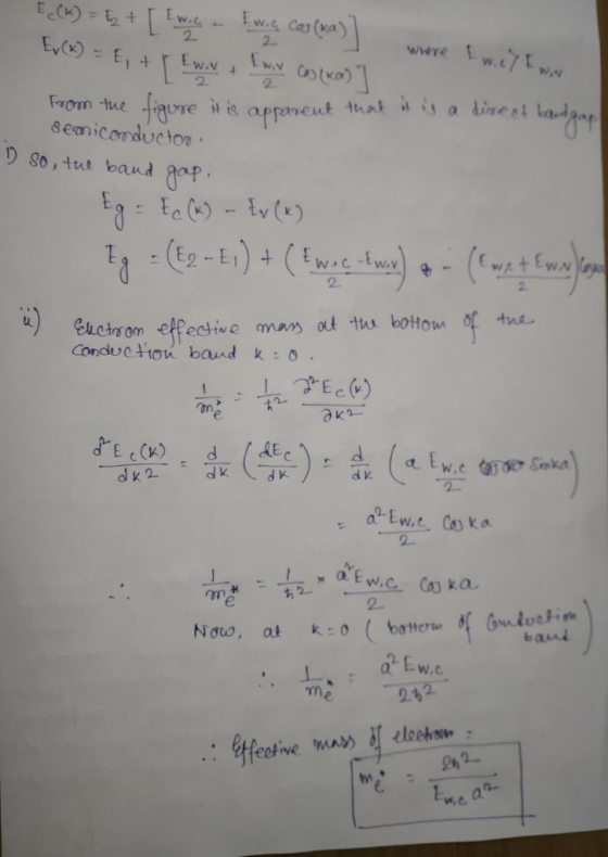
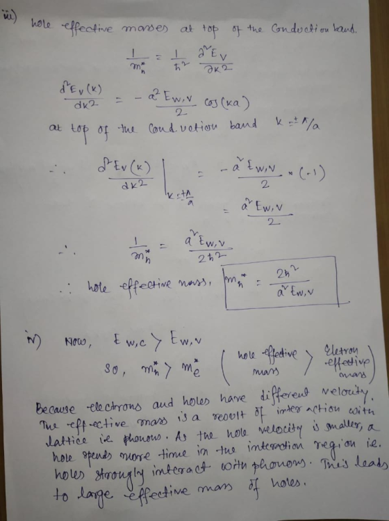
(Optional, 12 bonus points) Consider a imensional semiconductor with a band structure as shown in...
Band structure Consider a one-dimensional semiconductor crystal consisting of 11 atoms with nearest- neighbor atoms separated...
 Band structure Consider a one-dimensional semiconductor crystal consisting of 11 atoms with nearest- neighbor atoms separated by a 5 . The band structure for electrons in the conduction band is given by Ec(k) = 101(k-0.2n)2-A(k-02n)"] + 2.25 [eV] and the band structure for holes in the valence band is given by where the wavevector k s in units ofA-1. The allowed wavevectors are--< k 즈 al (a) Is this a direct or indirect gap semiconductor? What is the energy gap...
A) Show that the chemical potential in an intrinsic semiconductor lies in the middle of the gap a...
a) Show that the chemical potential in an intrinsic semiconductor lies in the middle of the gap at low temperature. (b) Explain how the chemical potential varies with temperature if the semiconductor is doped with (i) donors (ii) acceptors. (c) A direct-gap semiconductor is doped to produce a density of 1023electrons/m3. Calculate the hole density at room temperature given that the gap is 1.0 eV, and the effective mass of carriers in the conduction and valence band are 0.25 and...
The band structure of an unknown semiconductor is given by Ec (k) = 20k2 - 20k...
 The band structure of an unknown semiconductor is given by Ec (k) = 20k2 - 20k +6.5 [eV] Ey (k) = 6k2 + 0.6k - 0.065 [eV] where the wavevector k is measured in units of A-1. Assume room temperature. (a) Is this a direct-gap or an indirect-gap semiconductor? What is its energy gap? (15 points) (b) Determine the effective mass for electron and holes for this semiconductor. (10 points)
The band structure of an unknown semiconductor is given by...
The band structure of an unknown semiconductor is given by Ec (k) = 20k2 - 20k +6.5 [eV] Ey (k) = 6k2 + 0.6k - 0.065 [eV] where the wavevector k is measured in units of A-1. Assume room temperature. (a) Is this a direct-gap or an indirect-gap semiconductor? What is its energy gap? (15 points) (b) Determine the effective mass for electron and holes for this semiconductor. (10 points)
The band structure of an unknown semiconductor is given by...
The band structure of an unknown semiconductor is given by Ec (k) = 20k2 20k +6.5...
 The band structure of an unknown semiconductor is given by Ec (k) = 20k2 20k +6.5 [eV] Ey (k) = -6k2 +0.6k - 0.065 [eV] where the wavevector k is measured in units of A-1. Assume room temperature. (a) Is this a direct-gap or an indirect-gap semiconductor? What is its energy gap? (15 points) (b) Determine the effective mass for electron and holes for this semiconductor. (10 points)
The band structure of an unknown semiconductor is given by Ec (k)...
The band structure of an unknown semiconductor is given by Ec (k) = 20k2 20k +6.5 [eV] Ey (k) = -6k2 +0.6k - 0.065 [eV] where the wavevector k is measured in units of A-1. Assume room temperature. (a) Is this a direct-gap or an indirect-gap semiconductor? What is its energy gap? (15 points) (b) Determine the effective mass for electron and holes for this semiconductor. (10 points)
The band structure of an unknown semiconductor is given by Ec (k)...
A wire is made of an intrinsic semiconductor whose bandgap is 1.0eV. The wire is 0.05microns...
 A wire is made of an intrinsic semiconductor whose bandgap is 1.0eV. The wire is 0.05microns in diameter and 1 micron long. Electrons have a mobility of 1000/cm V-sec and holes have a mobility of 200/cm V-sec. The effective mass of an electron in the conduction band is 1.2 and that of a hole in the valence band is 0.6. The semiconductor operates at room temperature. a. What is the probability of finding an electron at an energy 0.5eV above...
semiconductor devices . Electron-hole recombination in direct band-gap semiconductors is known to yield photons. (0) For...
 semiconductor devices
. Electron-hole recombination in direct band-gap semiconductors is known to yield photons. (0) For which application this property is used? Explain briefly (ii) Calculate the primary wavelength of photons emitted from InP as a result of such recombination. (ii) Is it possible to see the emitted photons? Explain briefly (iv) Suppose you desire to detect the radiation from a GaP laser, can you use a Ge photodetector for that purpose? Explain briefly
semiconductor devices
. Electron-hole recombination in direct band-gap semiconductors is known to yield photons. (0) For which application this property is used? Explain briefly (ii) Calculate the primary wavelength of photons emitted from InP as a result of such recombination. (ii) Is it possible to see the emitted photons? Explain briefly (iv) Suppose you desire to detect the radiation from a GaP laser, can you use a Ge photodetector for that purpose? Explain briefly
Please explain part b in details thx! Question 2 At 300 K, the bandgap of GaP is 2.26 eV and the effective density of states at the conduction and valence band edge are 1.8 x 1019 cm23 and 1.9 x 10¹⁹...
 Please explain part b in details thx!
Question 2 At 300 K, the bandgap of GaP is 2.26 eV and the effective density of states at the conduction and valence band edge are 1.8 x 1019 cm23 and 1.9 x 1019 cm3, respectively. (a) Calculate the intrinsic concentration of GaP at 300K (7 marks) Calculate the GaP effective mass of holes at 300K. (b) (8 marks) (c The GaP sample is now doped with donor concentration of 1021 cm3 with...
Please explain part b in details thx!
Question 2 At 300 K, the bandgap of GaP is 2.26 eV and the effective density of states at the conduction and valence band edge are 1.8 x 1019 cm23 and 1.9 x 1019 cm3, respectively. (a) Calculate the intrinsic concentration of GaP at 300K (7 marks) Calculate the GaP effective mass of holes at 300K. (b) (8 marks) (c The GaP sample is now doped with donor concentration of 1021 cm3 with...
2. (a) Assuming Anderson's rule and Vegard's law calculate the depth of the confining potential in meV, for holes in the valence band of a InAs/InxGa1-xAs multi QW structure where x-0.5. [5]...
 2. (a) Assuming Anderson's rule and Vegard's law calculate the depth of the confining potential in meV, for holes in the valence band of a InAs/InxGa1-xAs multi QW structure where x-0.5. [5] State whether electron and hole confinement is within the InAs or InGaAs layers, and hence deduce what type of structure/band alignment this is. Suggest why this structure might be difficult to grow experimentally. (b) A Gao.47lno.53As quantum well laser is designed to emit at 1.55um at room temperature...
E(k)t Er K. 4. (Advanced Level) Graphene is a special type of material which is two- dimensional and has a linear E...
 E(k)t Er K. 4. (Advanced Level) Graphene is a special type of material which is two- dimensional and has a linear E-k diagram. The conduction and valence bands touch each other at a singularity, known as the Dirac point. In the unexcited state, the valence band is completely filled, while the conduction band is completely empty From the E-k diagram shown above, deduce the equation of the E-k curve. Hence, from the equation you deduced, speculate the special properties of...
helpp Problem 5b. - 10 Points total A semiconductor material has an energy gap of 0.75...
 helpp
Problem 5b. - 10 Points total A semiconductor material has an energy gap of 0.75 eV, effective masses mn= 0.04 mo and mp= 0.22 mo, where mo is the free electron mass = 9.11 x 10³ [kg]. Assume complete ionization. a) Let the temperature be T = 350 °K. The material is un-doped. Find the intrinsic Fermi level EFi and carrier concentration ni- pi (4 points) b) Let the temperature be T = 350 K. The material is doped...
helpp
Problem 5b. - 10 Points total A semiconductor material has an energy gap of 0.75 eV, effective masses mn= 0.04 mo and mp= 0.22 mo, where mo is the free electron mass = 9.11 x 10³ [kg]. Assume complete ionization. a) Let the temperature be T = 350 °K. The material is un-doped. Find the intrinsic Fermi level EFi and carrier concentration ni- pi (4 points) b) Let the temperature be T = 350 K. The material is doped...
 Band structure Consider a one-dimensional semiconductor crystal consisting of 11 atoms with nearest- neighbor atoms separated by a 5 . The band structure for electrons in the conduction band is given by Ec(k) = 101(k-0.2n)2-A(k-02n)"] + 2.25 [eV] and the band structure for holes in the valence band is given by where the wavevector k s in units ofA-1. The allowed wavevectors are--< k 즈 al (a) Is this a direct or indirect gap semiconductor? What is the energy gap...
 The band structure of an unknown semiconductor is given by Ec (k) = 20k2 - 20k +6.5 [eV] Ey (k) = 6k2 + 0.6k - 0.065 [eV] where the wavevector k is measured in units of A-1. Assume room temperature. (a) Is this a direct-gap or an indirect-gap semiconductor? What is its energy gap? (15 points) (b) Determine the effective mass for electron and holes for this semiconductor. (10 points)
The band structure of an unknown semiconductor is given by...
The band structure of an unknown semiconductor is given by Ec (k) = 20k2 - 20k +6.5 [eV] Ey (k) = 6k2 + 0.6k - 0.065 [eV] where the wavevector k is measured in units of A-1. Assume room temperature. (a) Is this a direct-gap or an indirect-gap semiconductor? What is its energy gap? (15 points) (b) Determine the effective mass for electron and holes for this semiconductor. (10 points)
The band structure of an unknown semiconductor is given by...
 The band structure of an unknown semiconductor is given by Ec (k) = 20k2 20k +6.5 [eV] Ey (k) = -6k2 +0.6k - 0.065 [eV] where the wavevector k is measured in units of A-1. Assume room temperature. (a) Is this a direct-gap or an indirect-gap semiconductor? What is its energy gap? (15 points) (b) Determine the effective mass for electron and holes for this semiconductor. (10 points)
The band structure of an unknown semiconductor is given by Ec (k)...
The band structure of an unknown semiconductor is given by Ec (k) = 20k2 20k +6.5 [eV] Ey (k) = -6k2 +0.6k - 0.065 [eV] where the wavevector k is measured in units of A-1. Assume room temperature. (a) Is this a direct-gap or an indirect-gap semiconductor? What is its energy gap? (15 points) (b) Determine the effective mass for electron and holes for this semiconductor. (10 points)
The band structure of an unknown semiconductor is given by Ec (k)...
 A wire is made of an intrinsic semiconductor whose bandgap is 1.0eV. The wire is 0.05microns in diameter and 1 micron long. Electrons have a mobility of 1000/cm V-sec and holes have a mobility of 200/cm V-sec. The effective mass of an electron in the conduction band is 1.2 and that of a hole in the valence band is 0.6. The semiconductor operates at room temperature. a. What is the probability of finding an electron at an energy 0.5eV above...
 semiconductor devices
. Electron-hole recombination in direct band-gap semiconductors is known to yield photons. (0) For which application this property is used? Explain briefly (ii) Calculate the primary wavelength of photons emitted from InP as a result of such recombination. (ii) Is it possible to see the emitted photons? Explain briefly (iv) Suppose you desire to detect the radiation from a GaP laser, can you use a Ge photodetector for that purpose? Explain briefly
semiconductor devices
. Electron-hole recombination in direct band-gap semiconductors is known to yield photons. (0) For which application this property is used? Explain briefly (ii) Calculate the primary wavelength of photons emitted from InP as a result of such recombination. (ii) Is it possible to see the emitted photons? Explain briefly (iv) Suppose you desire to detect the radiation from a GaP laser, can you use a Ge photodetector for that purpose? Explain briefly
 Please explain part b in details thx!
Question 2 At 300 K, the bandgap of GaP is 2.26 eV and the effective density of states at the conduction and valence band edge are 1.8 x 1019 cm23 and 1.9 x 1019 cm3, respectively. (a) Calculate the intrinsic concentration of GaP at 300K (7 marks) Calculate the GaP effective mass of holes at 300K. (b) (8 marks) (c The GaP sample is now doped with donor concentration of 1021 cm3 with...
Please explain part b in details thx!
Question 2 At 300 K, the bandgap of GaP is 2.26 eV and the effective density of states at the conduction and valence band edge are 1.8 x 1019 cm23 and 1.9 x 1019 cm3, respectively. (a) Calculate the intrinsic concentration of GaP at 300K (7 marks) Calculate the GaP effective mass of holes at 300K. (b) (8 marks) (c The GaP sample is now doped with donor concentration of 1021 cm3 with...
 2. (a) Assuming Anderson's rule and Vegard's law calculate the depth of the confining potential in meV, for holes in the valence band of a InAs/InxGa1-xAs multi QW structure where x-0.5. [5] State whether electron and hole confinement is within the InAs or InGaAs layers, and hence deduce what type of structure/band alignment this is. Suggest why this structure might be difficult to grow experimentally. (b) A Gao.47lno.53As quantum well laser is designed to emit at 1.55um at room temperature...
 E(k)t Er K. 4. (Advanced Level) Graphene is a special type of material which is two- dimensional and has a linear E-k diagram. The conduction and valence bands touch each other at a singularity, known as the Dirac point. In the unexcited state, the valence band is completely filled, while the conduction band is completely empty From the E-k diagram shown above, deduce the equation of the E-k curve. Hence, from the equation you deduced, speculate the special properties of...
 helpp
Problem 5b. - 10 Points total A semiconductor material has an energy gap of 0.75 eV, effective masses mn= 0.04 mo and mp= 0.22 mo, where mo is the free electron mass = 9.11 x 10³ [kg]. Assume complete ionization. a) Let the temperature be T = 350 °K. The material is un-doped. Find the intrinsic Fermi level EFi and carrier concentration ni- pi (4 points) b) Let the temperature be T = 350 K. The material is doped...
helpp
Problem 5b. - 10 Points total A semiconductor material has an energy gap of 0.75 eV, effective masses mn= 0.04 mo and mp= 0.22 mo, where mo is the free electron mass = 9.11 x 10³ [kg]. Assume complete ionization. a) Let the temperature be T = 350 °K. The material is un-doped. Find the intrinsic Fermi level EFi and carrier concentration ni- pi (4 points) b) Let the temperature be T = 350 K. The material is doped...
Most questions answered within 3 hours.
-
Describe the content of the queue and the output of the
following series of queue operations...
asked 58 seconds from now -
Why is a cell non able to function normally once it passes S
phase of interphase?...
asked 3 minutes ago -
What is the molecular shape and the electronic geometry of CCl3,
H3O, CO3, and SO2?
asked 19 minutes ago -
a cylinder contains 10 moles of an ideal gas at a temperature of
300 K. The...
asked 17 minutes ago -
Consider a value to be significantly low if its z score less
than or equal to...
asked 24 minutes ago -
Consider the reaction:
SO2Cl2(g)⇌SO2(g)+Cl2(g) Kp=2.91×10³ at 298 K
In a reaction at equilibrium, the partial pressure...
asked 24 minutes ago -
QUESTION 17
The wavelength of blue light is comparable to the size of
A.
At atomic...
asked 27 minutes ago -
Ball 1, with a mass of 120 g and traveling at 11 m/s , collides
head...
asked 31 minutes ago -
This question is about calculating and printing
payslips. User inputs his name, number of worked hours...
asked 32 minutes ago -
What is an interaction style and what is its role in effective
interface design? List and...
asked 40 minutes ago -
EXPLAIN HOW THIS PROGRAM WORKS, USING DEV C++
#include <iostream>
#include <cmath>
#define PI 3.1415926535897
using...
asked 51 minutes ago -
In the method below, add code to return the index of the element
in array that...
asked 1 hour ago