
Homework Answers


Add Answer to:
it is ECE 345 course
A. Look through the sections on various BJT voltage amplifier configurations...
The Final Project for the ELECTRONICS-1 course for, consists of designing a cascaded BJT Amplifier; using...
 The Final Project for the ELECTRONICS-1 course for, consists of
designing a cascaded BJT Amplifier; using 2 stages. The first stage
will be the Common Emitter (CE) Amplifier, the second stage is the
Common Collector (CC) Amplifier, as shown in the general diagram
below:
The overall amplification (voltage gain) Atotal =
98
The input source voltage Vsource is
an ideal source(Rs=0 Ohm) with peak voltage 10 mV,
and the source frequency
fsource =2K Hz
The load resistance RL = 47...
The Final Project for the ELECTRONICS-1 course for, consists of
designing a cascaded BJT Amplifier; using 2 stages. The first stage
will be the Common Emitter (CE) Amplifier, the second stage is the
Common Collector (CC) Amplifier, as shown in the general diagram
below:
The overall amplification (voltage gain) Atotal =
98
The input source voltage Vsource is
an ideal source(Rs=0 Ohm) with peak voltage 10 mV,
and the source frequency
fsource =2K Hz
The load resistance RL = 47...
Given the multistage amplifier below, select all correct statements Multistage-Amp Group of answer choices The collector...
Given the multistage amplifier below, select all correct statements Multistage-Amp Group of answer choices The collector current in Q2 is approximately 16mA The input impedance of the amplifier is approximately 2.5Megohms The output impedance of the amplifier (assuming Q2) has a Beta=100 is close to 500Kohms The overall gain for the circuit (including loading effects) is approximately 13 If an overall gain for the multistage amplifier of 20 is desired, RG can be selected around 450 to account for any...
Avec Úvo SRE L V II. (5pt) Consider the above-right common-collector or emitter-follower BJT amplifier circuit....
 Avec Úvo SRE L V II. (5pt) Consider the above-right common-collector or emitter-follower BJT amplifier circuit. Given: ß= 100, RE = 10 k1, Vcc = 20 V, RB = 5 k1, R1 = 10 kl, and Ry = 2 k1. (a) (1pt) Find the Q-point, i.e. Ibo, Ico, and VCEO; (b) (1pt) draw the small-signal equivalent circuit assuming that the capacitors (C, and Cy) are short circuits for the small signal; (c) (1pt) solve for the voltage gain, Av; (d)...
We design a voltage amplifier using a BJT following the plan laid down in the handout "Notes on common emitter...
 We design a voltage amplifier using a BJT following the plan laid down in the handout "Notes on common emitter transistor amplifier 8 IN RB Design an amplifier with a Gain VoutVinl30 Assume the transistor gain is B 100. Let Vcc 15 V Choose VCE Vcc-VCE.Sat Choose Ic.o-10 mA. 1. Determine values of resistors Rc, RE, and RB so that the gain is essentially independent of the value of β 2. State and satisfy the load-line relation between lc.a and...
100 1.5 0.27 5. 6 Pl. Consider the CB amplifier of Figure 1, for which Vcc-15...
 100 1.5 0.27 5. 6 Pl. Consider the CB amplifier of Figure 1, for which Vcc-15 V, Rs-50 Ω, and RL-10 kQ. For the BJT, assume that B150, VBE.on0.7 V, and VcE,sat 0.3 V, and ignore the Early effect. For the other resistances, however, assume the same values as those you used for the Common-Emitter (CE) amplifier lab (disregard the value for RE2, as the resistor does not exist in the CB amplifier of Figure 1). Therefore, copy the same...
Calculate the voltage gain (Av) for the loaded Common Emitter Amplifier below: BAC 200 for all...
 Calculate the voltage gain (Av) for the loaded Common Emitter Amplifier below: BAC 200 for all transistors. Assume re 15 Q for the CE Amplifier. Ignore re' for the DP Amplifier Vcc 12 V, R1 56 K, R2 10 KQ, R4 22 KQ R3 5.6 KQ, RL 8 RE(CE) 628 0, RE(CC) 330 Rc 3.5 KQ, Enter your results. No units. SR3 R1 RC C3 Vcc C1 Beta Q2a HH Vin Beta Q1 Beta Q2b C4 R4 Vs R2 C2...
What you want more? BJT Amplifier Design Final Project Requirements: The Final Project consists of designing...
 What you want more?
BJT Amplifier Design Final Project Requirements: The Final Project consists of designing a cascaded BJT Amplifier, using 2 stages. The first stage will be the Common Emitter (CE) Amplifier, the second stage is the Common Collector (CC) Amplifier, as shown in the general diagram below: CE → cc The design requirements are described here: The overall amplification (voltage gain) Axotal as given to each student (each student has different total voltage gain Atotal value] The input...
What you want more?
BJT Amplifier Design Final Project Requirements: The Final Project consists of designing a cascaded BJT Amplifier, using 2 stages. The first stage will be the Common Emitter (CE) Amplifier, the second stage is the Common Collector (CC) Amplifier, as shown in the general diagram below: CE → cc The design requirements are described here: The overall amplification (voltage gain) Axotal as given to each student (each student has different total voltage gain Atotal value] The input...
A common-emitter BJT amplificr is shown in Fig.8.1. Note the DC biasing values and the BJTsmall-s...
 A common-emitter BJT amplificr is shown in Fig.8.1. Note the DC biasing values and the BJTsmall-signalmodel parameters from the class-signment #9 on DC Bia ing. Neglect the value of Rs in your calculations, k1 Rs-a k2: 1· Cal ulatethesmall-agalpannetas ofthe amplifi randcompletethecalculated valuesinTable8-1 Smalls-signal voltage gai, AVk Small-signal input resistance,k, Small-signaloutput resistance, Ro VW RC 2k C2 RB 570k Rs C1 1 10uP 0.1m 1 Vs CE RE 2k SINE(0 1mV 1kHz 0 0 00) tran 0 2ms 0 1us...
1.0 kn. RE-390 Ω, r-15 Ω. and ßac-75. 5. For a common-emitter amplifier, Rc Assuming that Rg is completely bypassed at the operating frequency, the voltage gain is (a) 66.7 (d) 75 (b) 2.56 (c) 2....
 1.0 kn. RE-390 Ω, r-15 Ω. and ßac-75. 5. For a common-emitter amplifier, Rc Assuming that Rg is completely bypassed at the operating frequency, the voltage gain is (a) 66.7 (d) 75 (b) 2.56 (c) 2.47 6. In the circuit of Question 5, if the frequency is reduced to the point where Xctbypass) RE, the voltage gain (a) remains the same (b) is less (c) is greater 7. In a common-emitter amplifier with voltage-divider bias, Rimlbase) 68 k2, Ri 33...
Electronics1. It's a multiple choices question. use the formula sheet if needed (the last picture). Question...
 Electronics1. It's a multiple choices question. use the formula
sheet if needed (the last picture).
Question 9 CIRCUIT X/FIG.9 (5 Marks) Statement: Consider the RC-coupled amplifier circuit illustrated in Fig. 9 (CIRCUIT X). Sketching relevant output (V-I) characteristics that decide Q-point coordinates and DC load-line details of the NPN-BJT/Si circuit of Fig. 9 of Circuit x) Further, establish an appropriate AC-load line and decide the maximum swing of the output voltage across Road with respect to the Q-point. Assume the...
Electronics1. It's a multiple choices question. use the formula
sheet if needed (the last picture).
Question 9 CIRCUIT X/FIG.9 (5 Marks) Statement: Consider the RC-coupled amplifier circuit illustrated in Fig. 9 (CIRCUIT X). Sketching relevant output (V-I) characteristics that decide Q-point coordinates and DC load-line details of the NPN-BJT/Si circuit of Fig. 9 of Circuit x) Further, establish an appropriate AC-load line and decide the maximum swing of the output voltage across Road with respect to the Q-point. Assume the...
 The Final Project for the ELECTRONICS-1 course for, consists of
designing a cascaded BJT Amplifier; using 2 stages. The first stage
will be the Common Emitter (CE) Amplifier, the second stage is the
Common Collector (CC) Amplifier, as shown in the general diagram
below:
The overall amplification (voltage gain) Atotal =
98
The input source voltage Vsource is
an ideal source(Rs=0 Ohm) with peak voltage 10 mV,
and the source frequency
fsource =2K Hz
The load resistance RL = 47...
The Final Project for the ELECTRONICS-1 course for, consists of
designing a cascaded BJT Amplifier; using 2 stages. The first stage
will be the Common Emitter (CE) Amplifier, the second stage is the
Common Collector (CC) Amplifier, as shown in the general diagram
below:
The overall amplification (voltage gain) Atotal =
98
The input source voltage Vsource is
an ideal source(Rs=0 Ohm) with peak voltage 10 mV,
and the source frequency
fsource =2K Hz
The load resistance RL = 47...
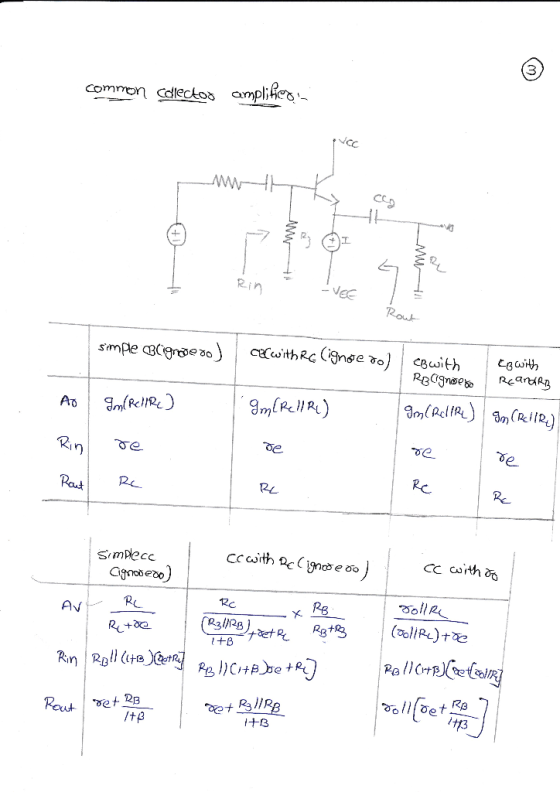
 Avec Úvo SRE L V II. (5pt) Consider the above-right common-collector or emitter-follower BJT amplifier circuit. Given: ß= 100, RE = 10 k1, Vcc = 20 V, RB = 5 k1, R1 = 10 kl, and Ry = 2 k1. (a) (1pt) Find the Q-point, i.e. Ibo, Ico, and VCEO; (b) (1pt) draw the small-signal equivalent circuit assuming that the capacitors (C, and Cy) are short circuits for the small signal; (c) (1pt) solve for the voltage gain, Av; (d)...
 We design a voltage amplifier using a BJT following the plan laid down in the handout "Notes on common emitter transistor amplifier 8 IN RB Design an amplifier with a Gain VoutVinl30 Assume the transistor gain is B 100. Let Vcc 15 V Choose VCE Vcc-VCE.Sat Choose Ic.o-10 mA. 1. Determine values of resistors Rc, RE, and RB so that the gain is essentially independent of the value of β 2. State and satisfy the load-line relation between lc.a and...
 100 1.5 0.27 5. 6 Pl. Consider the CB amplifier of Figure 1, for which Vcc-15 V, Rs-50 Ω, and RL-10 kQ. For the BJT, assume that B150, VBE.on0.7 V, and VcE,sat 0.3 V, and ignore the Early effect. For the other resistances, however, assume the same values as those you used for the Common-Emitter (CE) amplifier lab (disregard the value for RE2, as the resistor does not exist in the CB amplifier of Figure 1). Therefore, copy the same...
 Calculate the voltage gain (Av) for the loaded Common Emitter Amplifier below: BAC 200 for all transistors. Assume re 15 Q for the CE Amplifier. Ignore re' for the DP Amplifier Vcc 12 V, R1 56 K, R2 10 KQ, R4 22 KQ R3 5.6 KQ, RL 8 RE(CE) 628 0, RE(CC) 330 Rc 3.5 KQ, Enter your results. No units. SR3 R1 RC C3 Vcc C1 Beta Q2a HH Vin Beta Q1 Beta Q2b C4 R4 Vs R2 C2...
 What you want more?
BJT Amplifier Design Final Project Requirements: The Final Project consists of designing a cascaded BJT Amplifier, using 2 stages. The first stage will be the Common Emitter (CE) Amplifier, the second stage is the Common Collector (CC) Amplifier, as shown in the general diagram below: CE → cc The design requirements are described here: The overall amplification (voltage gain) Axotal as given to each student (each student has different total voltage gain Atotal value] The input...
What you want more?
BJT Amplifier Design Final Project Requirements: The Final Project consists of designing a cascaded BJT Amplifier, using 2 stages. The first stage will be the Common Emitter (CE) Amplifier, the second stage is the Common Collector (CC) Amplifier, as shown in the general diagram below: CE → cc The design requirements are described here: The overall amplification (voltage gain) Axotal as given to each student (each student has different total voltage gain Atotal value] The input...
 A common-emitter BJT amplificr is shown in Fig.8.1. Note the DC biasing values and the BJTsmall-signalmodel parameters from the class-signment #9 on DC Bia ing. Neglect the value of Rs in your calculations, k1 Rs-a k2: 1· Cal ulatethesmall-agalpannetas ofthe amplifi randcompletethecalculated valuesinTable8-1 Smalls-signal voltage gai, AVk Small-signal input resistance,k, Small-signaloutput resistance, Ro VW RC 2k C2 RB 570k Rs C1 1 10uP 0.1m 1 Vs CE RE 2k SINE(0 1mV 1kHz 0 0 00) tran 0 2ms 0 1us...
 1.0 kn. RE-390 Ω, r-15 Ω. and ßac-75. 5. For a common-emitter amplifier, Rc Assuming that Rg is completely bypassed at the operating frequency, the voltage gain is (a) 66.7 (d) 75 (b) 2.56 (c) 2.47 6. In the circuit of Question 5, if the frequency is reduced to the point where Xctbypass) RE, the voltage gain (a) remains the same (b) is less (c) is greater 7. In a common-emitter amplifier with voltage-divider bias, Rimlbase) 68 k2, Ri 33...
 Electronics1. It's a multiple choices question. use the formula
sheet if needed (the last picture).
Question 9 CIRCUIT X/FIG.9 (5 Marks) Statement: Consider the RC-coupled amplifier circuit illustrated in Fig. 9 (CIRCUIT X). Sketching relevant output (V-I) characteristics that decide Q-point coordinates and DC load-line details of the NPN-BJT/Si circuit of Fig. 9 of Circuit x) Further, establish an appropriate AC-load line and decide the maximum swing of the output voltage across Road with respect to the Q-point. Assume the...
Electronics1. It's a multiple choices question. use the formula
sheet if needed (the last picture).
Question 9 CIRCUIT X/FIG.9 (5 Marks) Statement: Consider the RC-coupled amplifier circuit illustrated in Fig. 9 (CIRCUIT X). Sketching relevant output (V-I) characteristics that decide Q-point coordinates and DC load-line details of the NPN-BJT/Si circuit of Fig. 9 of Circuit x) Further, establish an appropriate AC-load line and decide the maximum swing of the output voltage across Road with respect to the Q-point. Assume the...
Most questions answered within 3 hours.
-
Find the area of the shaded region. The graph to the right
depicts IQ scores of...
asked 2 minutes ago -
A spring is characterized by a spring constant of 60 N/m. How
much potential energy does...
asked 3 minutes ago -
strategic hr:
Devise staffing strategies for the following organizations:
Church based soup kitchen staffed with volunteers...
asked 6 minutes ago -
1887, Barnes, a physician living in Carlilse, Cumberland NW
England reports on a case of food...
asked 6 minutes ago -
Residents of two states were surveyed regarding whether or not
they were fans of professional football...
asked 19 minutes ago -
A study was done to compare the amount of time per day students
at public and...
asked 26 minutes ago -
For regularization, we added the regularizer to the loss
function. Does it make sense to multiply...
asked 32 minutes ago -
b. A freezer you got from a student sale has an inside
temperature of – 10C;...
asked 34 minutes ago -
PEARSON
Years
S&P 500
Stock Price
2014
1,692
$68.00
2015
1,978
$102.00
2016
1,884
$110.00
2017...
asked 35 minutes ago -
You roll a fair 6-sided dice, let Y be the outcome of the dice
roll. Then...
asked 1 hour ago -
If the value of the range is equal to zero, then this indicates
that:
A. there...
asked 1 hour ago -
Based on Simms' (1994) articulation of psychological privacy to
promote development of self-identity, for example, do...
asked 47 minutes ago