
Homework Answers
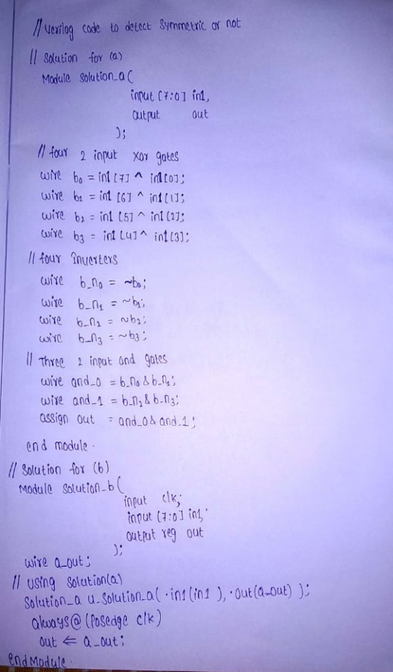
![Il solution for (1) Module Solution input ck, input (7:0] ini, output reg out wiXC Q_out; reg delay_flop; ll using Solution (](http://img.homeworklib.com/questions/ddf9ca00-c0ac-11ea-94fc-d3320973a6f3.png?x-oss-process=image/resize,w_560)
Add Answer to:
1&2 and please I need quickly.
Q1 (35 pts): Design a combinational circuit that takes 8...
3. (10 Points) RTL Combinational Circuit Design a Draw the schematic for the Verilog code given...
 3. (10 Points) RTL Combinational Circuit Design a Draw the schematic for the Verilog code given below: module abc (a, b, c, d, si, s0); input 31, 30; output a, b, c,d; not (51_, 51), (50_, 0); and (a, s1_, SO_); and (b, s1_, 0); and (c, sl, s0_); and (d, sl, s0); endmodule b. Draw the schematic for the Verilog code given below: module Always_Code input a, b, c, output reg F ); always @(a, b, c) begin F...
Please help to complete the code and write the testbench to design the following adder. 1.In...
Please help to complete the code and write the testbench to design the following adder. 1.In this section, you add pipeline stage. 8 bits are used at every pipeline stage.Use the following template to complete your Verilog coding. // Addition of two 16 bit, 2's complement nos., n1 and n2. 8 bits addition at a time. Result is 17 bits. module adder_b (clk, n1, n2, sum) ; input clk ; input [15:0] n1 ; input [15:0] n2 ; output [16:0]...
Consider the circuit in Figure 1. It is a 4-bit (QQ2Q3) synchronous counter which uses four T-typ...
 Consider the circuit in Figure 1. It is a 4-bit (QQ2Q3) synchronous counter which uses four T-type flip-flops. The counter increases its value on each positive edge of the clock if the Enable signal is asserted. The counter is reset to 0 by setting the Clear signal low. You are to implement an 8-bit counter of this type Enable T Q Clock Clear Figure 1. 4-bit synchronous counter (but you need to implement 8-bit counter in this lab) Specific notes:...
I need help writing a test bench for the following Verilog code module CU(IE, WE, WA,...
I need help writing a test bench for the following Verilog code module CU(IE, WE, WA, RAE, RAA, RBE, RBA, ALU, SH, OE, start, clk, reset, Ng5); //nG5 denotes (N>5); input start, clk, reset; output IE, WE, RAE, RBE, OE; output [1:0] WA, RAA, RBA, SH; output [2:0] ALU; input wire Ng5; reg [1:0] state; reg [1:0] nextstate; parameter S0 = 3'b000; parameter S1 = 3'b001;...
I need the following in verilog. Attached is also the test bench. CODE // Design a...
I need the following in verilog. Attached is also the test bench. CODE // Design a circuit that divides a 4-bit signed binary number (in) // by 3 to produce a 3-bit signed binary number (out). Note that // integer division rounds toward zero for both positive and negative // numbers (e.g., -5/3 is -1). module sdiv3(out, in); output [2:0] out; input [3:0] in; endmodule // sdiv3 TEST BENCH module test; // these are inputs to "circuit under test" reg...
1. a. Design and implement a combinational circuit with three inputs w, x, and y and three outputs A, B and C using CMOS transistors. When the binary input is 0, 1, 2 or 3 the binary output is three g...
 1.
a. Design and implement a combinational circuit with three
inputs w, x, and y and three outputs A, B and C using CMOS
transistors. When the binary input is 0, 1, 2 or 3 the binary
output is three greater than the input. When the binary input is 4,
5, 6 or 7 the binary output is three less than the input.
b. from the part (a) , Draw the mask layout with Ln = Lp= 0.6
μm, Wn=...
1.
a. Design and implement a combinational circuit with three
inputs w, x, and y and three outputs A, B and C using CMOS
transistors. When the binary input is 0, 1, 2 or 3 the binary
output is three greater than the input. When the binary input is 4,
5, 6 or 7 the binary output is three less than the input.
b. from the part (a) , Draw the mask layout with Ln = Lp= 0.6
μm, Wn=...
In this lab, you will design a finite state machine to control the tail lights of...
 In this lab, you will design a finite state machine to control the tail lights of an unsual car. There are three lights on each side that operate in sequence to indicate thedirection of a turn. Figure ! shows the tail lights and Figure 2 shows the flashing sequence for (a) left turns and (b) right rums. ZOTTAS Figure 28:8: BCECECece BCECECECes BCECECECB BCECECBCB 8888 Figure 2 Part 1 - FSM Design Start with designing the state transition diagram for...
could you please help me with this problem, also I need a little text so I...
 could you please help me with this problem, also I
need a little text so I can understand how you solved the
problem?
import java.io.File; import java.util.Scanner; /** *
This program lists the files in a directory specified by * the
user. The user is asked to type in a directory name. * If the name
entered by the user is not a directory, a * message is printed and
the program ends. */ public class DirectoryList { public static...
could you please help me with this problem, also I
need a little text so I can understand how you solved the
problem?
import java.io.File; import java.util.Scanner; /** *
This program lists the files in a directory specified by * the
user. The user is asked to type in a directory name. * If the name
entered by the user is not a directory, a * message is printed and
the program ends. */ public class DirectoryList { public static...
 3. (10 Points) RTL Combinational Circuit Design a Draw the schematic for the Verilog code given below: module abc (a, b, c, d, si, s0); input 31, 30; output a, b, c,d; not (51_, 51), (50_, 0); and (a, s1_, SO_); and (b, s1_, 0); and (c, sl, s0_); and (d, sl, s0); endmodule b. Draw the schematic for the Verilog code given below: module Always_Code input a, b, c, output reg F ); always @(a, b, c) begin F...
 Consider the circuit in Figure 1. It is a 4-bit (QQ2Q3) synchronous counter which uses four T-type flip-flops. The counter increases its value on each positive edge of the clock if the Enable signal is asserted. The counter is reset to 0 by setting the Clear signal low. You are to implement an 8-bit counter of this type Enable T Q Clock Clear Figure 1. 4-bit synchronous counter (but you need to implement 8-bit counter in this lab) Specific notes:...
 1.
a. Design and implement a combinational circuit with three
inputs w, x, and y and three outputs A, B and C using CMOS
transistors. When the binary input is 0, 1, 2 or 3 the binary
output is three greater than the input. When the binary input is 4,
5, 6 or 7 the binary output is three less than the input.
b. from the part (a) , Draw the mask layout with Ln = Lp= 0.6
μm, Wn=...
1.
a. Design and implement a combinational circuit with three
inputs w, x, and y and three outputs A, B and C using CMOS
transistors. When the binary input is 0, 1, 2 or 3 the binary
output is three greater than the input. When the binary input is 4,
5, 6 or 7 the binary output is three less than the input.
b. from the part (a) , Draw the mask layout with Ln = Lp= 0.6
μm, Wn=...
 In this lab, you will design a finite state machine to control the tail lights of an unsual car. There are three lights on each side that operate in sequence to indicate thedirection of a turn. Figure ! shows the tail lights and Figure 2 shows the flashing sequence for (a) left turns and (b) right rums. ZOTTAS Figure 28:8: BCECECece BCECECECes BCECECECB BCECECBCB 8888 Figure 2 Part 1 - FSM Design Start with designing the state transition diagram for...
 could you please help me with this problem, also I
need a little text so I can understand how you solved the
problem?
import java.io.File; import java.util.Scanner; /** *
This program lists the files in a directory specified by * the
user. The user is asked to type in a directory name. * If the name
entered by the user is not a directory, a * message is printed and
the program ends. */ public class DirectoryList { public static...
could you please help me with this problem, also I
need a little text so I can understand how you solved the
problem?
import java.io.File; import java.util.Scanner; /** *
This program lists the files in a directory specified by * the
user. The user is asked to type in a directory name. * If the name
entered by the user is not a directory, a * message is printed and
the program ends. */ public class DirectoryList { public static...
Most questions answered within 3 hours.
-
Calculate the following: ***SHOW ALL WORK!!!! Or
NO CREDIT*** Circle your answers. 8pts
each
In the...
asked 48 minutes ago -
Bank Z is currently advertising interest rates on its checking
account. They claim to pay an...
asked 11 minutes ago -
List two ways of transformation on the response variable that
can be used to deal with...
asked 1 hour ago -
If a 2000 ohm resistor has a -3.90 mA current going through it.
What is the...
asked 1 hour ago -
Please comment on the sentences.
Some types of jobs require more training than others. Some
companies...
asked 2 hours ago -
The )G01 for the hydrolysis of phosphorarginine
reaction depicted below is –32 kJ mol-1.
Phosphoarginine ...
asked 2 hours ago -
Cross a heterozygous blue-eyed goat with a homozygous brown-eyed
goat. Be sure to indicate which kids...
asked 3 hours ago -
Use the following information to answer the next two
questions.
Please refer to question 9-90. A...
asked 3 hours ago -
A solution containing 0.050 g of an unknown electrolyte in 2.50
g of cyclohexane was found...
asked 3 hours ago -
Question 1
a) Hydraulic conductivity of soils is an important parameter for
the design of engineering...
asked 3 hours ago -
Suppose your credit card balance is
$15,000
The minimum payment is
$313
and the annual percentage...
asked 3 hours ago -
Professor plays basketball and makes 75% of free
throws she shoots. If professor shot 5 free...
asked 3 hours ago