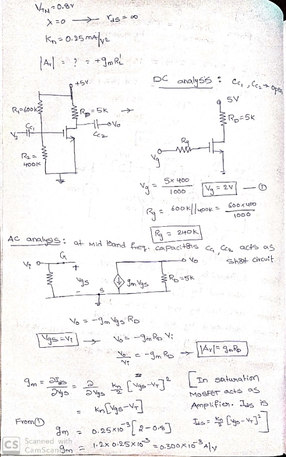
For the transistor in the circuit shown below, VTN = 0.8 V, lambda = 0, and Kn = 0.25 mA/V2. Determine the small-signal voltage gain of the circuit.

Homework Answers

Add Answer to:
For the transistor in the circuit shown below, VTN =
0.8 V, lambda = 0, and...
In the circuit in Figure P3.26, the transistor parameters are VTN = 0.8 V and Kn = 0.5 mA/V2.
 In the circuit in Figure P3.26, the transistor parameters are VTN = 0.8 V and Kn = 0.5 mA/V2. Calculate VGS, ID, and VDS.
For the circuit shown below, the transistor parameters are given as VTP - 0.8 V and...
 For the circuit shown below, the transistor parameters are given as VTP - 0.8 V and Kp = 200 MAN Find VSD 1 = 0.4 mA RG = 50 k 2 Rp=5 kn OOOO 2.2 v O 3V 5.2V -0.8V
Part 1/2 Consider the circuit shown in Figure 1, where RD = 1kQ, Vtn-0.9V, μ. Cox...
 Part 1/2 Consider the circuit shown in Figure 1, where RD = 1kQ, Vtn-0.9V, μ. Cox (W/L) = 1.5 mA/V and 2 0. Perform DC analysis to compute the voltages Vi and V2. -2.5V Figure 1 Part 2/2 Compute the small-signal voltage gain voVsi. Hints to the solution 1. Redraw the circuit in the AC small-signal domain as shown below, Roy 2. Find the small-signal equivalent Thevenin resistance seen between the source of M2 and the ground node, Re, indicated...
This is a very important assignment of mine please do it correctly I will give you...
 This is a very important assignment of mine please do it
correctly I will give you thumbs up
Problem 1. The transistor in the circuit shown to the
right has parameters VTN = 0.4 V, Kn =
= 0.5 mA / V2, and λ
= 0. The circuit parameters are VDD = 3 V and
Ri = R1||R2 = 300 kΩ.
a)Determine the values of R1, R2, and
RS such that IDQ = 0.25 mA and
VDSQ = 1.5 V....
This is a very important assignment of mine please do it
correctly I will give you thumbs up
Problem 1. The transistor in the circuit shown to the
right has parameters VTN = 0.4 V, Kn =
= 0.5 mA / V2, and λ
= 0. The circuit parameters are VDD = 3 V and
Ri = R1||R2 = 300 kΩ.
a)Determine the values of R1, R2, and
RS such that IDQ = 0.25 mA and
VDSQ = 1.5 V....
and Vpp = 18 V - Cc2 w S R = 500 k2 SRL W Žr...
 and Vpp = 18 V - Cc2 w S R = 500 k2 SRL W Žr {Rs -ov Figure P4.27 Figure P4.26 For the common-source amplifier shown in Figure P4.27, the transistor arameters are Vip = -1.2 V, Ko = 2 mA/V2, and 2 = 0.03 V-1. The iconductor Devices and Basic Applications drain resistor is Rp = 4k92. (a) Determine lo such that VSDQ = 5 V. (b) Find the small-signal voltage gain for RL = 00. (c) Repeat...
In a small signal voltage amplifier using a pnp transistor shown below, the voltage gain is 350.2. The value of a-0.95. Find the equivalent model emitter resistance re in Ohms if Rc-4.1K2. The BJT is...
 In a small signal voltage amplifier using a pnp transistor shown below, the voltage gain is 350.2. The value of a-0.95. Find the equivalent model emitter resistance re in Ohms if Rc-4.1K2. The BJT is operating at room temperature and VBE 0.7V RE-10K CCI vi Cc2 Rc
In a small signal voltage amplifier using a pnp transistor shown below, the voltage gain is 350.2. The value of a-0.95. Find the equivalent model emitter resistance re in Ohms if Rc-4.1K2. The...
In a small signal voltage amplifier using a pnp transistor shown below, the voltage gain is 350.2. The value of a-0.95. Find the equivalent model emitter resistance re in Ohms if Rc-4.1K2. The BJT is operating at room temperature and VBE 0.7V RE-10K CCI vi Cc2 Rc
In a small signal voltage amplifier using a pnp transistor shown below, the voltage gain is 350.2. The value of a-0.95. Find the equivalent model emitter resistance re in Ohms if Rc-4.1K2. The...
18.2 V, V-1.3 V and R, 1.6 Calculate Vds for the following circuit given that V kohms. Assume that the transistor threshold voltage is 0.8 volts and K is 2.51 mA/V. Hint: The transistor is in the sat...
 18.2 V, V-1.3 V and R, 1.6 Calculate Vds for the following circuit given that V kohms. Assume that the transistor threshold voltage is 0.8 volts and K is 2.51 mA/V. Hint: The transistor is in the saturation (constant current) region. +Vs Id ds
18.2 V, V-1.3 V and R, 1.6 Calculate Vds for the following circuit given that V kohms. Assume that the transistor threshold voltage is 0.8 volts and K is 2.51 mA/V. Hint: The transistor is in...
18.2 V, V-1.3 V and R, 1.6 Calculate Vds for the following circuit given that V kohms. Assume that the transistor threshold voltage is 0.8 volts and K is 2.51 mA/V. Hint: The transistor is in the saturation (constant current) region. +Vs Id ds
18.2 V, V-1.3 V and R, 1.6 Calculate Vds for the following circuit given that V kohms. Assume that the transistor threshold voltage is 0.8 volts and K is 2.51 mA/V. Hint: The transistor is in...
In the circuit of given below, Vsig is a small sine wave signal with zero average. The transistor...
 In the circuit of given below, Vsig is a small sine wave signal with zero average. The transistor B is 100. a) Find the value of RE to establish a dc emitter current of about 0.5 mA. b) Find Rc to establish a dc collector voltage of about +5 V c) For RL10 kS2 and the transistor ro 200 k2, draw the small-signal equivalent circuit 5. of the amplifier and determine its overall voltage gain +15 V Re O Vo...
ENG 301 Electronics I Homework 2 1 Refer to Figure 1. Assume ß 50 and VBE(on)...
 ENG 301 Electronics I Homework 2 1 Refer to Figure 1. Assume ß 50 and VBE(on) 0.7 V for all BJTs in the circuit. For Ri 12 kN and Rc 10 k2, find the differential voltage gain (Ad) of the differential amplifier taken as one- sided output at vc +10 V Rc +10 V IREPR -10 V Figure 1 2. Vcc +12 V RCI= 10 k2 R3= 15 k2 67.3 k2 Ris Cci Q1 Cc2 CC3 R4= 45 k2 R2...
QUESTION (1) Transistor Mi in this common base amplifier circuit has the following characteristics: +Vc VTH...
 QUESTION (1) Transistor Mi in this common base amplifier circuit has the following characteristics: +Vc VTH =1 V Rp R, C. K 1 mA/V2 2 0.1 R Given: Vcc 2 mA, 10 V, lbias Ct C2 0, 5 k2, RD 2 k2 RI 10 k, R2 R (12 points) a) Determine the small signal gain, vo/Vin. (4 points) b) Determine the input resistance, Rin. (4 points) c) Determine the output resistance, Ro. Useful formulae: for n-channel MOSFET triode region =...
 For the circuit shown below, the transistor parameters are given as VTP - 0.8 V and Kp = 200 MAN Find VSD 1 = 0.4 mA RG = 50 k 2 Rp=5 kn OOOO 2.2 v O 3V 5.2V -0.8V
 Part 1/2 Consider the circuit shown in Figure 1, where RD = 1kQ, Vtn-0.9V, μ. Cox (W/L) = 1.5 mA/V and 2 0. Perform DC analysis to compute the voltages Vi and V2. -2.5V Figure 1 Part 2/2 Compute the small-signal voltage gain voVsi. Hints to the solution 1. Redraw the circuit in the AC small-signal domain as shown below, Roy 2. Find the small-signal equivalent Thevenin resistance seen between the source of M2 and the ground node, Re, indicated...
 This is a very important assignment of mine please do it
correctly I will give you thumbs up
Problem 1. The transistor in the circuit shown to the
right has parameters VTN = 0.4 V, Kn =
= 0.5 mA / V2, and λ
= 0. The circuit parameters are VDD = 3 V and
Ri = R1||R2 = 300 kΩ.
a)Determine the values of R1, R2, and
RS such that IDQ = 0.25 mA and
VDSQ = 1.5 V....
This is a very important assignment of mine please do it
correctly I will give you thumbs up
Problem 1. The transistor in the circuit shown to the
right has parameters VTN = 0.4 V, Kn =
= 0.5 mA / V2, and λ
= 0. The circuit parameters are VDD = 3 V and
Ri = R1||R2 = 300 kΩ.
a)Determine the values of R1, R2, and
RS such that IDQ = 0.25 mA and
VDSQ = 1.5 V....
 and Vpp = 18 V - Cc2 w S R = 500 k2 SRL W Žr {Rs -ov Figure P4.27 Figure P4.26 For the common-source amplifier shown in Figure P4.27, the transistor arameters are Vip = -1.2 V, Ko = 2 mA/V2, and 2 = 0.03 V-1. The iconductor Devices and Basic Applications drain resistor is Rp = 4k92. (a) Determine lo such that VSDQ = 5 V. (b) Find the small-signal voltage gain for RL = 00. (c) Repeat...
 In a small signal voltage amplifier using a pnp transistor shown below, the voltage gain is 350.2. The value of a-0.95. Find the equivalent model emitter resistance re in Ohms if Rc-4.1K2. The BJT is operating at room temperature and VBE 0.7V RE-10K CCI vi Cc2 Rc
In a small signal voltage amplifier using a pnp transistor shown below, the voltage gain is 350.2. The value of a-0.95. Find the equivalent model emitter resistance re in Ohms if Rc-4.1K2. The...
In a small signal voltage amplifier using a pnp transistor shown below, the voltage gain is 350.2. The value of a-0.95. Find the equivalent model emitter resistance re in Ohms if Rc-4.1K2. The BJT is operating at room temperature and VBE 0.7V RE-10K CCI vi Cc2 Rc
In a small signal voltage amplifier using a pnp transistor shown below, the voltage gain is 350.2. The value of a-0.95. Find the equivalent model emitter resistance re in Ohms if Rc-4.1K2. The...
 18.2 V, V-1.3 V and R, 1.6 Calculate Vds for the following circuit given that V kohms. Assume that the transistor threshold voltage is 0.8 volts and K is 2.51 mA/V. Hint: The transistor is in the saturation (constant current) region. +Vs Id ds
18.2 V, V-1.3 V and R, 1.6 Calculate Vds for the following circuit given that V kohms. Assume that the transistor threshold voltage is 0.8 volts and K is 2.51 mA/V. Hint: The transistor is in...
18.2 V, V-1.3 V and R, 1.6 Calculate Vds for the following circuit given that V kohms. Assume that the transistor threshold voltage is 0.8 volts and K is 2.51 mA/V. Hint: The transistor is in the saturation (constant current) region. +Vs Id ds
18.2 V, V-1.3 V and R, 1.6 Calculate Vds for the following circuit given that V kohms. Assume that the transistor threshold voltage is 0.8 volts and K is 2.51 mA/V. Hint: The transistor is in...
 In the circuit of given below, Vsig is a small sine wave signal with zero average. The transistor B is 100. a) Find the value of RE to establish a dc emitter current of about 0.5 mA. b) Find Rc to establish a dc collector voltage of about +5 V c) For RL10 kS2 and the transistor ro 200 k2, draw the small-signal equivalent circuit 5. of the amplifier and determine its overall voltage gain +15 V Re O Vo...
 ENG 301 Electronics I Homework 2 1 Refer to Figure 1. Assume ß 50 and VBE(on) 0.7 V for all BJTs in the circuit. For Ri 12 kN and Rc 10 k2, find the differential voltage gain (Ad) of the differential amplifier taken as one- sided output at vc +10 V Rc +10 V IREPR -10 V Figure 1 2. Vcc +12 V RCI= 10 k2 R3= 15 k2 67.3 k2 Ris Cci Q1 Cc2 CC3 R4= 45 k2 R2...
 QUESTION (1) Transistor Mi in this common base amplifier circuit has the following characteristics: +Vc VTH =1 V Rp R, C. K 1 mA/V2 2 0.1 R Given: Vcc 2 mA, 10 V, lbias Ct C2 0, 5 k2, RD 2 k2 RI 10 k, R2 R (12 points) a) Determine the small signal gain, vo/Vin. (4 points) b) Determine the input resistance, Rin. (4 points) c) Determine the output resistance, Ro. Useful formulae: for n-channel MOSFET triode region =...
Most questions answered within 3 hours.
-
The average length of time between arrivals at a turnpike
toll-booth is 26 seconds. What is...
asked 12 minutes ago -
(a) A piston at 6.1 atm contains a gas that occupies a volume of
3.5 L....
asked 1 hour ago -
Please answer true or false. Words
cannot be changed or added in to make it true...
asked 1 hour ago -
An empty test tube weighs 15.923 grams. Then,
MgCl2•6H2O is added into the test tube. After...
asked 1 hour ago -
Assume memory access is 10 units of time and disk access is
10000 units of time....
asked 1 hour ago -
1. Are all good samples random?
2. Magazines often report surveys giving statistics such as “63%...
asked 2 hours ago -
Under all the various types of market structures, firms
must eventually earn some economic profits for...
asked 1 hour ago -
Consider the following fitness regime for a single locus trait
with two co-dominant alleles: w11 =...
asked 1 hour ago -
A large cable company reports the following.
80% of its customers subscribe to its cable TV...
asked 2 hours ago -
Please answer the question in brief.
Discuss the role of ERP in organizations. Are ERP tools...
asked 1 hour ago -
Discuss the pros and cons of collaborative software such
as SameTime. Does it increase productivity? What...
asked 2 hours ago -
Buying your in-laws a gift because it’s expected is
due to the ____________ motive of gift-giving....
asked 2 hours ago