The following is an equivalent way of creating the circuit above.
![D[2] DIUI D[O D Flip Flop Flip Flop sw_in on sw in sw in clock clock clock 0121 0111 Q[o]](http://img.homeworklib.com/questions/6e2388e0-0974-11eb-872b-81196a31a8c5.png?x-oss-process=image/resize,w_560)
Below is the truth table
Q2, Q1, and Q0 are LED outputs from left to right respectively and D2, D1, and D0 are switches from left to right respectively
Answer the following questions:
1. What signal(s) represent the present state and next state of the circuit?
2. Sketch a Finite State Machine diagram of the circuit (Be sure to show inputs and outputs).
3. Describe the high-level behavior of the circuit (what does it do?)
4. Given the function of the circuit, what does the state of the circuit represent?
Homework Answers
Answer 1:
the signals that represent the present state.
(these are those signals which give the output of flip flop at the current clock cycle)
hence, Q0,Q1,Q2 are present state variables.
the next state variables are:
the variables that define what will be the next state of the FSM. when the next clock pulse arrives.
hence next state variables are D0,D1,D2
answer 2.)

answer 3:
the circuit has an output taken from
Q2,Q1,Q0.
from the table given and the state diagram we see that the value is binary is counting up. until it reaches 111 and then reverts back to 0 every time a clock pulse arrives.
hence the circuit is counting clock pulses. hence the circuit is an 3 bit Synchronous up counter.
answer 4:
the current state of the above circuit represents the number of clock cycles which has passed or supplied to the circuit in range from 0-7.
counting up.
hence the circuit is called an up counter.
Add Answer to:
The following is an equivalent way of creating the circuit
above.
Below is the truth table...
The following three images accompany one another. The second image is another version of the first...
 The following three images accompany one another. The second
image is another version of the first which we are using in the
example. How does image 4 change the function of the circuit (an
input, 'a', has been added that logically influences the next state
bits)?? Fill out the truth table to show the change.
Note: Q2, Q1, and Q0 are LED outputs from left to right
respectively. D2, D1, and D0 are switches from left to right
respectively. 'a'...
The following three images accompany one another. The second
image is another version of the first which we are using in the
example. How does image 4 change the function of the circuit (an
input, 'a', has been added that logically influences the next state
bits)?? Fill out the truth table to show the change.
Note: Q2, Q1, and Q0 are LED outputs from left to right
respectively. D2, D1, and D0 are switches from left to right
respectively. 'a'...
Also explain in words what this means. Assuming that Q2 Q1 and Q0 are LEDs from...
 Also explain in words what this means. Assuming that Q2 Q1 and
Q0 are LEDs from left to right respectively, and D2, D1, and D0 are
switches from left to right respectively. Just explain a few states
for my understanding.
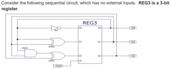
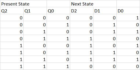
Consider the following sequential circuit, which has no external inputs. REG3 is a 3-bit register. REG3 DO 00 00 DI 01 Q1 XORZ AND2 D2 02 Q2 XORZ clk clock Present State Next State Q2 Q1 QO D2 D1 DO...
Also explain in words what this means. Assuming that Q2 Q1 and
Q0 are LEDs from left to right respectively, and D2, D1, and D0 are
switches from left to right respectively. Just explain a few states
for my understanding.
Consider the following sequential circuit, which has no external inputs. REG3 is a 3-bit register. REG3 DO 00 00 DI 01 Q1 XORZ AND2 D2 02 Q2 XORZ clk clock Present State Next State Q2 Q1 QO D2 D1 DO...
In Verilog, design the circuit below (an upcounter) using 3 D flip flops shown in image2....
 In Verilog, design the circuit below (an upcounter) using 3 D
flip flops shown in image2. To be programmed in Vivado and used on
BASYS3 board
REG3 DO 20 QO DI 01 21 XORZ AND2 D2 Q2 Q2 XORZ cik clock D[2] D[11 DIO D Flip-Flop Flip Flop swin en sw in sw_in clock clock clock 0[2] [11 Q[o]
In Verilog, design the circuit below (an upcounter) using 3 D
flip flops shown in image2. To be programmed in Vivado and used on
BASYS3 board
REG3 DO 20 QO DI 01 21 XORZ AND2 D2 Q2 Q2 XORZ cik clock D[2] D[11 DIO D Flip-Flop Flip Flop swin en sw in sw_in clock clock clock 0[2] [11 Q[o]
What is the function of this circuit? It is a sequential circuit with no external inputs....
 What is the function of this circuit? It is a sequential circuit
with no external inputs. Draw a schematic using the Flip-Flop
diagram below that performs the task it is intended to. The design
will eventually be programmed to an FPGA board.
REG3 DO 00 QO DI 01 101 XORZ AND2 02 02 Q2 XOR2 cik clock D[2] D[1] D[O] D Flip-Flop Flip-Flop Flip-Flop sw_in en sw_in sw_in clock clock clock Q[2] Q[1] Q[o]
What is the function of this circuit? It is a sequential circuit
with no external inputs. Draw a schematic using the Flip-Flop
diagram below that performs the task it is intended to. The design
will eventually be programmed to an FPGA board.
REG3 DO 00 QO DI 01 101 XORZ AND2 02 02 Q2 XOR2 cik clock D[2] D[1] D[O] D Flip-Flop Flip-Flop Flip-Flop sw_in en sw_in sw_in clock clock clock Q[2] Q[1] Q[o]
Consider a 4-bit binary counter that increments on every clock pulse. (a) Construct the state diagram for a counter that has an state variable word A3A2A1A0. (b) Construct the state table by assuming...
Consider a 4-bit binary counter that increments on every clock pulse. (a) Construct the state diagram for a counter that has an state variable word A3A2A1A0. (b) Construct the state table by assuming that the circuit consists of four D-type flip-flops with the inputs D3, D2, D1, D0 corresponding to the outputs A3, A2, A1, A0, respectively. (c) Determine the Boolean equations for the flip-flop inputs as functions of the state variables A3, A2, A1, A0, respectively. (d) Design the...
Design a 3- bit Multipurpose Register. The register utilizes 3 "D" type flip flops with outputs...
Design a 3- bit Multipurpose Register. The register utilizes 3 "D" type flip flops with outputs Q0, Q1, Q2. The Registers has a synchronous clock input(CLK) that clocks all 3 flip flops on its positive edge The Registers has an asynchronous clear input(CLR' ) that sets all flip flops to "0" when active low. The Register has 2 select inputs, S0 and S1 that selects the functions as folows: S1 = 0, 0, 1, 1 and S0 = 0,1,0,1 and...
The task is to design a two-bit controlled counter which has two counting bits (Q2, Q1), has one control input C1, and a...
 The task is to design a two-bit controlled counter which has two
counting bits (Q2, Q1), has one control input C1, and also two
extra outputs, one indicating overflow, the other underflow.
When C1=0 the counter counts up by 2s; i.e. 0 becomes 2, 1
becomes 3. In this mode the values 2 and 3 go to the overflow
state. When the control input C1=1, the counter counts down by 2s,
i.e. 3 becomes 1, and 2 becomes 0, and...
The task is to design a two-bit controlled counter which has two
counting bits (Q2, Q1), has one control input C1, and also two
extra outputs, one indicating overflow, the other underflow.
When C1=0 the counter counts up by 2s; i.e. 0 becomes 2, 1
becomes 3. In this mode the values 2 and 3 go to the overflow
state. When the control input C1=1, the counter counts down by 2s,
i.e. 3 becomes 1, and 2 becomes 0, and...
A combination circuit is specified by the following Boolean functions listed below. h(a, b, c) = b,c' + a'c Implement the circuit with a 3x8 decoder. Provide truth table and drawing the l...
 A combination circuit is specified by the following Boolean functions listed below. h(a, b, c) = b,c' + a'c Implement the circuit with a 3x8 decoder. Provide truth table and drawing the logic/circuit diagram. Use the block diagram for the decoder provided in Figure A4 in supplements. Please label the inputs and outputs clearly. Note: use single 3x8 decoder Question 2 (15 points] A priority encoder is an encoder circuit that includes the Truth Table of a priority function. The...
Design a counter to count-up from 2 to 5 using 3 D Flip-Flops similar to the...
 Design a counter to count-up from 2 to 5 using 3 D Flip-Flops similar to the following sample: Important Steps: After you simplify D2, D1 and DO by kmap Have a piece of paper to draw it then open iCircuit to design it using BCD If it works well as a counter, copy the design from iCircuit and paste it here. 3-Bit Counter Using D Flip-Flop: The State Equation of D Flip-Flop: Q(t+1)=D(t) => Dn=An Count Up From 3 To...
Show all steps C- For the following circuit, find the state and the outputs of the...
 Show all steps
C- For the following circuit, find the state and the outputs of the flip flops for three clocks. Assume that all flip flops are initially (A = 1, B = 1) and the input x = 0. Clock statc J-K flip flop J-K flip flop state A|A | state BB Initial state Clock Clock Clock
Show all steps
C- For the following circuit, find the state and the outputs of the flip flops for three clocks. Assume that all flip flops are initially (A = 1, B = 1) and the input x = 0. Clock statc J-K flip flop J-K flip flop state A|A | state BB Initial state Clock Clock Clock
 The following three images accompany one another. The second
image is another version of the first which we are using in the
example. How does image 4 change the function of the circuit (an
input, 'a', has been added that logically influences the next state
bits)?? Fill out the truth table to show the change.
Note: Q2, Q1, and Q0 are LED outputs from left to right
respectively. D2, D1, and D0 are switches from left to right
respectively. 'a'...
The following three images accompany one another. The second
image is another version of the first which we are using in the
example. How does image 4 change the function of the circuit (an
input, 'a', has been added that logically influences the next state
bits)?? Fill out the truth table to show the change.
Note: Q2, Q1, and Q0 are LED outputs from left to right
respectively. D2, D1, and D0 are switches from left to right
respectively. 'a'...
 Also explain in words what this means. Assuming that Q2 Q1 and
Q0 are LEDs from left to right respectively, and D2, D1, and D0 are
switches from left to right respectively. Just explain a few states
for my understanding.
Consider the following sequential circuit, which has no external inputs. REG3 is a 3-bit register. REG3 DO 00 00 DI 01 Q1 XORZ AND2 D2 02 Q2 XORZ clk clock Present State Next State Q2 Q1 QO D2 D1 DO...
Also explain in words what this means. Assuming that Q2 Q1 and
Q0 are LEDs from left to right respectively, and D2, D1, and D0 are
switches from left to right respectively. Just explain a few states
for my understanding.
Consider the following sequential circuit, which has no external inputs. REG3 is a 3-bit register. REG3 DO 00 00 DI 01 Q1 XORZ AND2 D2 02 Q2 XORZ clk clock Present State Next State Q2 Q1 QO D2 D1 DO...
 In Verilog, design the circuit below (an upcounter) using 3 D
flip flops shown in image2. To be programmed in Vivado and used on
BASYS3 board
REG3 DO 20 QO DI 01 21 XORZ AND2 D2 Q2 Q2 XORZ cik clock D[2] D[11 DIO D Flip-Flop Flip Flop swin en sw in sw_in clock clock clock 0[2] [11 Q[o]
In Verilog, design the circuit below (an upcounter) using 3 D
flip flops shown in image2. To be programmed in Vivado and used on
BASYS3 board
REG3 DO 20 QO DI 01 21 XORZ AND2 D2 Q2 Q2 XORZ cik clock D[2] D[11 DIO D Flip-Flop Flip Flop swin en sw in sw_in clock clock clock 0[2] [11 Q[o]
 What is the function of this circuit? It is a sequential circuit
with no external inputs. Draw a schematic using the Flip-Flop
diagram below that performs the task it is intended to. The design
will eventually be programmed to an FPGA board.
REG3 DO 00 QO DI 01 101 XORZ AND2 02 02 Q2 XOR2 cik clock D[2] D[1] D[O] D Flip-Flop Flip-Flop Flip-Flop sw_in en sw_in sw_in clock clock clock Q[2] Q[1] Q[o]
What is the function of this circuit? It is a sequential circuit
with no external inputs. Draw a schematic using the Flip-Flop
diagram below that performs the task it is intended to. The design
will eventually be programmed to an FPGA board.
REG3 DO 00 QO DI 01 101 XORZ AND2 02 02 Q2 XOR2 cik clock D[2] D[1] D[O] D Flip-Flop Flip-Flop Flip-Flop sw_in en sw_in sw_in clock clock clock Q[2] Q[1] Q[o]
 The task is to design a two-bit controlled counter which has two
counting bits (Q2, Q1), has one control input C1, and also two
extra outputs, one indicating overflow, the other underflow.
When C1=0 the counter counts up by 2s; i.e. 0 becomes 2, 1
becomes 3. In this mode the values 2 and 3 go to the overflow
state. When the control input C1=1, the counter counts down by 2s,
i.e. 3 becomes 1, and 2 becomes 0, and...
The task is to design a two-bit controlled counter which has two
counting bits (Q2, Q1), has one control input C1, and also two
extra outputs, one indicating overflow, the other underflow.
When C1=0 the counter counts up by 2s; i.e. 0 becomes 2, 1
becomes 3. In this mode the values 2 and 3 go to the overflow
state. When the control input C1=1, the counter counts down by 2s,
i.e. 3 becomes 1, and 2 becomes 0, and...
 A combination circuit is specified by the following Boolean functions listed below. h(a, b, c) = b,c' + a'c Implement the circuit with a 3x8 decoder. Provide truth table and drawing the logic/circuit diagram. Use the block diagram for the decoder provided in Figure A4 in supplements. Please label the inputs and outputs clearly. Note: use single 3x8 decoder Question 2 (15 points] A priority encoder is an encoder circuit that includes the Truth Table of a priority function. The...
 Design a counter to count-up from 2 to 5 using 3 D Flip-Flops similar to the following sample: Important Steps: After you simplify D2, D1 and DO by kmap Have a piece of paper to draw it then open iCircuit to design it using BCD If it works well as a counter, copy the design from iCircuit and paste it here. 3-Bit Counter Using D Flip-Flop: The State Equation of D Flip-Flop: Q(t+1)=D(t) => Dn=An Count Up From 3 To...
 Show all steps
C- For the following circuit, find the state and the outputs of the flip flops for three clocks. Assume that all flip flops are initially (A = 1, B = 1) and the input x = 0. Clock statc J-K flip flop J-K flip flop state A|A | state BB Initial state Clock Clock Clock
Show all steps
C- For the following circuit, find the state and the outputs of the flip flops for three clocks. Assume that all flip flops are initially (A = 1, B = 1) and the input x = 0. Clock statc J-K flip flop J-K flip flop state A|A | state BB Initial state Clock Clock Clock
Most questions answered within 3 hours.
-
A sample of n = 25 scores produces a t statistic of t =
-2.062. If...
asked 13 minutes ago -
Given the following, compute the after tax cost of debt: The par
value of the firms...
asked 7 minutes ago -
Coding in C. Please only use stdio.h (which would mean no malloc
or anything like that)...
asked 12 minutes ago -
Use the fundamental accounting equation to find the missing
amounts.
Scenario
Assets
Liabilities
Equity
1
$...
asked 11 minutes ago -
A population has a mean of 200 and a standard deviation of 60.
Suppose a sample...
asked 15 minutes ago -
A bicyclist starting at rest produces a constant angular
acceleration of 1.10 rad/s2 for wheels that...
asked 29 minutes ago -
The
half-life of a radioactive source is 14.0 minutes. How much time
must elapse before the...
asked 27 minutes ago -
Given P(Ec ) = 0.43, P(F) = 0.52, and P(EF) = 0.18.
Find P( E |...
asked 1 hour ago -
Consider two empty containers A and B whose volumes are
10mL and 20mL respectively. 1mL of...
asked 1 hour ago -
QUESTION 6
Determine the linear momentum of a 2,800 kg houseboat going 3
m/s.
9,100 kg.m/s...
asked 1 hour ago -
Jor-el throws a ball upward from the top of a 728 foot building
on the planet...
asked 1 hour ago -
Which of the following will most likely to happen if Federal
Reserve Bank decreases the money...
asked 1 hour ago