
Homework Answers

![Input Impedance Ri = vi Kul at tlp loop Y 0 -Vit hie If + (ithfe) IL RE, = 0 ni = H (hiet (l+hfelRfi] Ria - [hie+ (it hfe) Re](http://img.homeworklib.com/questions/eaebc5a0-4105-11eb-8d96-4bdc0bd1e158.png?x-oss-process=image/resize,w_560)

Add Answer to:
5. Determine the following parameters for the amplifier of figure 4. Assume B= 150 and VA-...
Q.A. 2 -Statement: DC biasing of a CE amplifier circuit is as in Fig.2 Assume the...
 Q.A. 2 -Statement: DC biasing of a CE amplifier
circuit is as in Fig.2 Assume the parameters, VCC
= 12 volt, RE = 450 ohm; = 100; RL = 2250 ohm, RC =1000 ohm and
source resistance and Rs = 2500 ohm. Also, the device emitter
resistance re is negligible.
The amplifier is excited by a source, vs(t) = Vm × sin(2ft)
with Vm = 500 mV peak and f = 5500 Hz; and, coupling and by-pass
capacitors can...
Q.A. 2 -Statement: DC biasing of a CE amplifier
circuit is as in Fig.2 Assume the parameters, VCC
= 12 volt, RE = 450 ohm; = 100; RL = 2250 ohm, RC =1000 ohm and
source resistance and Rs = 2500 ohm. Also, the device emitter
resistance re is negligible.
The amplifier is excited by a source, vs(t) = Vm × sin(2ft)
with Vm = 500 mV peak and f = 5500 Hz; and, coupling and by-pass
capacitors can...
4. For the amplifier in the figure below use the parameters in the table: +Vcc Re VBE- 0.7V, Ri- ...
 4. For the amplifier in the figure below use the parameters in the table: +Vcc Re VBE- 0.7V, Ri- 1002, R1-160k2, R2-320k2 R3-200k2, R6-40 k2, Rc-60k2, Vcc- 12V, Ry Do a) Draw the DC equivalent circuit and calculate the Q-point. c) Draw the AC equivalent circuit with the small signal model for the transistor. d) Calculate the voltage gain, Av-Vo/vi. Assume ro infinite. e) Draw the circuit to find the amplifier input resistance (Rin). Calculate Rin f Draw the circuit...
ECE 330 Electronics Homework #4 Name: 1. Determine the r-parameters for the transistor of the fig...
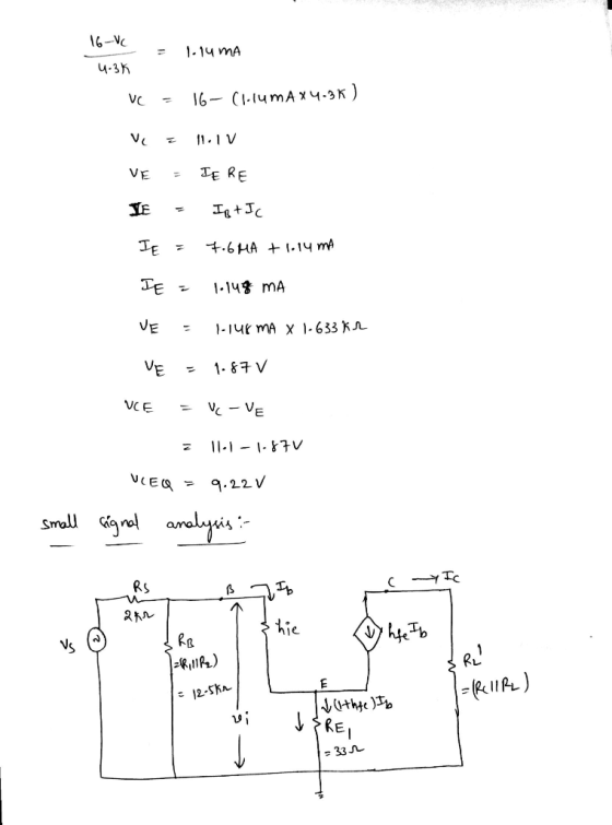
 ECE 330 Electronics Homework #4 Name: 1. Determine the r-parameters for the transistor of the figure below, and draw (15 points) signal equivalent circuit. Assume β 150 tlo Rs 10μF 2N2222A RI S 4.7 ks2 Determine all the parameters for the CE amplifier with gain stabilization shown below, using the approximate transistor model (neglecting the effect of ro) Vcc 16 V 4. (15 points) Assume β-160 Ri 30 kQ 2N3904 's100 mV Rg
ECE 330 Electronics Homework #4 Name: 1....
ECE 330 Electronics Homework #4 Name: 1. Determine the r-parameters for the transistor of the figure below, and draw (15 points) signal equivalent circuit. Assume β 150 tlo Rs 10μF 2N2222A RI S 4.7 ks2 Determine all the parameters for the CE amplifier with gain stabilization shown below, using the approximate transistor model (neglecting the effect of ro) Vcc 16 V 4. (15 points) Assume β-160 Ri 30 kQ 2N3904 's100 mV Rg
ECE 330 Electronics Homework #4 Name: 1....
5. Determine the Ico and Vceo for the emitter-biased common-emitter amplifier circuit show below. Assume B=180....
 5. Determine the Ico and Vceo for the emitter-biased common-emitter amplifier circuit show below. Assume B=180. (12 points) Vcc 918 v Rs12330 ks Rc 1,5 k22 Rs2 B V ce 18 220 ke2 RE 30.75 k2 6. Draw the circuit diagram of a common-emitter voltage-divider bias with the following parameters. (12 points) Vcc = 16V, R, -30k1, R2 = 10k22, Rc = 3.3kQ2, Re = 1.5k22, B = 199 (a) Determine lco and Vcro using the approximate method. (b) Determine...
For the circuit shown below, let Vcc 9 V R2 RE-0.11 kQ, R1 3.6 k2. and R2 -5.6 kQ. The transistor parameters are β-200, VBE(on)-OTV, VA-100 V and VT = 0.026 V. (a) Determine the quiescent value o...
 For the circuit shown below, let Vcc 9 V R2 RE-0.11 kQ, R1 3.6 k2. and R2 -5.6 kQ. The transistor parameters are β-200, VBE(on)-OTV, VA-100 V and VT = 0.026 V. (a) Determine the quiescent value of IEQ (b) Find the small-signal voltage gain Av Vo/vs (c) Determine the output resistance R, looking into output terminals Av= 0.5589 Ro-0.4688 Ω Ro-0.9118 Ω leQ- 23.76 mA Ra " 0.6538 Ω leo 39.52 mA A, 0.9938
For the circuit shown below,...
For the circuit shown below, let Vcc 9 V R2 RE-0.11 kQ, R1 3.6 k2. and R2 -5.6 kQ. The transistor parameters are β-200, VBE(on)-OTV, VA-100 V and VT = 0.026 V. (a) Determine the quiescent value of IEQ (b) Find the small-signal voltage gain Av Vo/vs (c) Determine the output resistance R, looking into output terminals Av= 0.5589 Ro-0.4688 Ω Ro-0.9118 Ω leQ- 23.76 mA Ra " 0.6538 Ω leo 39.52 mA A, 0.9938
For the circuit shown below,...
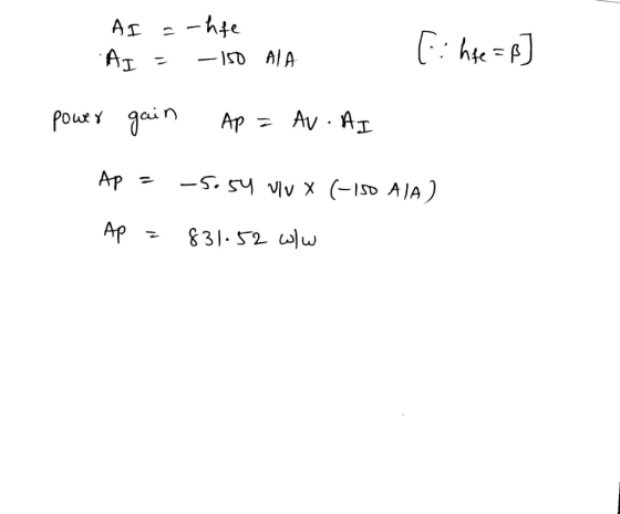
18. Determine the following ac values for the amplifier in Figure below. (c) A, (e) Ap...
 18. Determine the following ac values for the amplifier in Figure below. (c) A, (e) Ap (a) Rin (b) Rin(tot) (d) A¡ Vcc +18 V Rc 3.3 kn C2 ER 47 kN o Vout 104F βρC 75 10 mV B = 70 10μF C3 100 µF RE R, 12 k2 1.0 kN
The following Amplifier needs to be designed such that the voltage gain Av = 54. Assume...
 The following Amplifier needs to be designed such that the voltage gain Av = 54. Assume Vcc=10V, B=50, RL= 10 kq, RS = 100, and design for Ico= 0.48 mA and VEQ = 2V. (a) Find the values of Gm and it (b) Find the values of resistors R1, R2, RC, RE using the design procedure presented in class notes (or textbook) In the answer box write the value of Rc in ko (c) Find the Input resistance (d) Find...
For the following circuits, determine Av (Voutput/Vinput), Rin, and Rout. Given that threshold voltage (Vt) =...
 For the following circuits, determine Av (Voutput/Vinput), Rin, and Rout. Given that threshold voltage (Vt) = 1.65 V, early voltage (Va) = 51V, transconductance parameter Kn = un. COX. W/L = 0.5 mA/V2 Signal coupling capacitors are 47 uF, VDD =+9 V and VSS =-9V. The resistor values are RG= 1.5 MO, RD=20 kq, RS1 =1.8 k 2, RS2 =18 kl with RS =RS1 +RS2. - The load resistor is RL=47 ko. > lg 3 Roi Vou 3 R Xw2...
4. The amplifier shown below has Rsig-RL 1kQ. Rc 1kQ, RB 47 kQ. β 100, Cc1 a) Find the dc collect...
 4. The amplifier shown below has Rsig-RL 1kQ. Rc 1kQ, RB 47 kQ. β 100, Cc1 a) Find the dc collector current of the transistor b) Find gm and IT c) Neglecting ro, find the midband voltage gain from base to collector (neglect the effect of RB) d) Use the gain obtained in part (c) to find the component of Rin that arises as a result of RB. Hence find Rin. e) Find the overall gain at midband f) Find...
please I need details l and....Debate Club | Offic A) Theoretical Design Design a common emitter BJT amplifier with the following requirements: -Rin-10 K2, and Ro-45 ㏀ (Neglect the Early voltage...
 please I need details
l and....Debate Club | Offic A) Theoretical Design Design a common emitter BJT amplifier with the following requirements: -Rin-10 K2, and Ro-45 ㏀ (Neglect the Early voltage Effect) Vo/Vsig- Gv-40 VIV or 32 dB " VCC-9 V V, IC-1mA, VCE-3.25V and β-100 RL-40 kQ, Rsige I ka, R 1-3R2, and C1-C2-1 μF Voc RC C2 R1 Rsig C1 RL R2 RE B) Verify your design using Orcad Capture Pspice by doing 1) AC sweep (frequency response):...
please I need details
l and....Debate Club | Offic A) Theoretical Design Design a common emitter BJT amplifier with the following requirements: -Rin-10 K2, and Ro-45 ㏀ (Neglect the Early voltage Effect) Vo/Vsig- Gv-40 VIV or 32 dB " VCC-9 V V, IC-1mA, VCE-3.25V and β-100 RL-40 kQ, Rsige I ka, R 1-3R2, and C1-C2-1 μF Voc RC C2 R1 Rsig C1 RL R2 RE B) Verify your design using Orcad Capture Pspice by doing 1) AC sweep (frequency response):...
 Q.A. 2 -Statement: DC biasing of a CE amplifier
circuit is as in Fig.2 Assume the parameters, VCC
= 12 volt, RE = 450 ohm; = 100; RL = 2250 ohm, RC =1000 ohm and
source resistance and Rs = 2500 ohm. Also, the device emitter
resistance re is negligible.
The amplifier is excited by a source, vs(t) = Vm × sin(2ft)
with Vm = 500 mV peak and f = 5500 Hz; and, coupling and by-pass
capacitors can...
Q.A. 2 -Statement: DC biasing of a CE amplifier
circuit is as in Fig.2 Assume the parameters, VCC
= 12 volt, RE = 450 ohm; = 100; RL = 2250 ohm, RC =1000 ohm and
source resistance and Rs = 2500 ohm. Also, the device emitter
resistance re is negligible.
The amplifier is excited by a source, vs(t) = Vm × sin(2ft)
with Vm = 500 mV peak and f = 5500 Hz; and, coupling and by-pass
capacitors can...
 4. For the amplifier in the figure below use the parameters in the table: +Vcc Re VBE- 0.7V, Ri- 1002, R1-160k2, R2-320k2 R3-200k2, R6-40 k2, Rc-60k2, Vcc- 12V, Ry Do a) Draw the DC equivalent circuit and calculate the Q-point. c) Draw the AC equivalent circuit with the small signal model for the transistor. d) Calculate the voltage gain, Av-Vo/vi. Assume ro infinite. e) Draw the circuit to find the amplifier input resistance (Rin). Calculate Rin f Draw the circuit...
 ECE 330 Electronics Homework #4 Name: 1. Determine the r-parameters for the transistor of the figure below, and draw (15 points) signal equivalent circuit. Assume β 150 tlo Rs 10μF 2N2222A RI S 4.7 ks2 Determine all the parameters for the CE amplifier with gain stabilization shown below, using the approximate transistor model (neglecting the effect of ro) Vcc 16 V 4. (15 points) Assume β-160 Ri 30 kQ 2N3904 's100 mV Rg
ECE 330 Electronics Homework #4 Name: 1....
ECE 330 Electronics Homework #4 Name: 1. Determine the r-parameters for the transistor of the figure below, and draw (15 points) signal equivalent circuit. Assume β 150 tlo Rs 10μF 2N2222A RI S 4.7 ks2 Determine all the parameters for the CE amplifier with gain stabilization shown below, using the approximate transistor model (neglecting the effect of ro) Vcc 16 V 4. (15 points) Assume β-160 Ri 30 kQ 2N3904 's100 mV Rg
ECE 330 Electronics Homework #4 Name: 1....
 5. Determine the Ico and Vceo for the emitter-biased common-emitter amplifier circuit show below. Assume B=180. (12 points) Vcc 918 v Rs12330 ks Rc 1,5 k22 Rs2 B V ce 18 220 ke2 RE 30.75 k2 6. Draw the circuit diagram of a common-emitter voltage-divider bias with the following parameters. (12 points) Vcc = 16V, R, -30k1, R2 = 10k22, Rc = 3.3kQ2, Re = 1.5k22, B = 199 (a) Determine lco and Vcro using the approximate method. (b) Determine...
 For the circuit shown below, let Vcc 9 V R2 RE-0.11 kQ, R1 3.6 k2. and R2 -5.6 kQ. The transistor parameters are β-200, VBE(on)-OTV, VA-100 V and VT = 0.026 V. (a) Determine the quiescent value of IEQ (b) Find the small-signal voltage gain Av Vo/vs (c) Determine the output resistance R, looking into output terminals Av= 0.5589 Ro-0.4688 Ω Ro-0.9118 Ω leQ- 23.76 mA Ra " 0.6538 Ω leo 39.52 mA A, 0.9938
For the circuit shown below,...
For the circuit shown below, let Vcc 9 V R2 RE-0.11 kQ, R1 3.6 k2. and R2 -5.6 kQ. The transistor parameters are β-200, VBE(on)-OTV, VA-100 V and VT = 0.026 V. (a) Determine the quiescent value of IEQ (b) Find the small-signal voltage gain Av Vo/vs (c) Determine the output resistance R, looking into output terminals Av= 0.5589 Ro-0.4688 Ω Ro-0.9118 Ω leQ- 23.76 mA Ra " 0.6538 Ω leo 39.52 mA A, 0.9938
For the circuit shown below,...
 18. Determine the following ac values for the amplifier in Figure below. (c) A, (e) Ap (a) Rin (b) Rin(tot) (d) A¡ Vcc +18 V Rc 3.3 kn C2 ER 47 kN o Vout 104F βρC 75 10 mV B = 70 10μF C3 100 µF RE R, 12 k2 1.0 kN
 The following Amplifier needs to be designed such that the voltage gain Av = 54. Assume Vcc=10V, B=50, RL= 10 kq, RS = 100, and design for Ico= 0.48 mA and VEQ = 2V. (a) Find the values of Gm and it (b) Find the values of resistors R1, R2, RC, RE using the design procedure presented in class notes (or textbook) In the answer box write the value of Rc in ko (c) Find the Input resistance (d) Find...
 For the following circuits, determine Av (Voutput/Vinput), Rin, and Rout. Given that threshold voltage (Vt) = 1.65 V, early voltage (Va) = 51V, transconductance parameter Kn = un. COX. W/L = 0.5 mA/V2 Signal coupling capacitors are 47 uF, VDD =+9 V and VSS =-9V. The resistor values are RG= 1.5 MO, RD=20 kq, RS1 =1.8 k 2, RS2 =18 kl with RS =RS1 +RS2. - The load resistor is RL=47 ko. > lg 3 Roi Vou 3 R Xw2...
 4. The amplifier shown below has Rsig-RL 1kQ. Rc 1kQ, RB 47 kQ. β 100, Cc1 a) Find the dc collector current of the transistor b) Find gm and IT c) Neglecting ro, find the midband voltage gain from base to collector (neglect the effect of RB) d) Use the gain obtained in part (c) to find the component of Rin that arises as a result of RB. Hence find Rin. e) Find the overall gain at midband f) Find...
 please I need details
l and....Debate Club | Offic A) Theoretical Design Design a common emitter BJT amplifier with the following requirements: -Rin-10 K2, and Ro-45 ㏀ (Neglect the Early voltage Effect) Vo/Vsig- Gv-40 VIV or 32 dB " VCC-9 V V, IC-1mA, VCE-3.25V and β-100 RL-40 kQ, Rsige I ka, R 1-3R2, and C1-C2-1 μF Voc RC C2 R1 Rsig C1 RL R2 RE B) Verify your design using Orcad Capture Pspice by doing 1) AC sweep (frequency response):...
please I need details
l and....Debate Club | Offic A) Theoretical Design Design a common emitter BJT amplifier with the following requirements: -Rin-10 K2, and Ro-45 ㏀ (Neglect the Early voltage Effect) Vo/Vsig- Gv-40 VIV or 32 dB " VCC-9 V V, IC-1mA, VCE-3.25V and β-100 RL-40 kQ, Rsige I ka, R 1-3R2, and C1-C2-1 μF Voc RC C2 R1 Rsig C1 RL R2 RE B) Verify your design using Orcad Capture Pspice by doing 1) AC sweep (frequency response):...
Most questions answered within 3 hours.
-
Suppose we have a binomial experiment in which success is
defined to be a particular quality...
asked 13 minutes ago -
march the type of cellular control with the description: enzyme
induction and the enzyme repression. How...
asked 23 minutes ago -
Brief Exercise 5-09 (Part Level Submission)
The following information relates to Blue Spruce Corp. for the...
asked 23 minutes ago -
An unknown amount of a compound with a molecular mass of 284.04
g/mol is dissolved in...
asked 28 minutes ago -
You are at rest at a stop sign. There is another stop sign that
is 100...
asked 29 minutes ago -
Calculate the equilibrium electrode potential for Fe3+/Fe2+
redox system, if the initial concentration of Fe2+ is...
asked 33 minutes ago -
Describe in detail with graph and diagram how bonding force,
bonding curves and bonding energy at...
asked 50 minutes ago -
Gingerbread cookies become inedible if not eaten quickly enough.
Clarence is trying to determine how many...
asked 45 minutes ago -
A
crane lifts a 200 kg block a height of 10 m in 18 seconds. What...
asked 48 minutes ago -
A 12.0-g bullet is fired horizontally into a 115-g wooden block
that is initially at rest...
asked 49 minutes ago -
Which DNA primer would have the HIGHEST melting temperature?
Question 17 options:
a)
GCATCGGC
b)
AATCGGAT...
asked 57 minutes ago -
what is the charge on the chromium ion in Cr2O3.
a -3
b -2
c 0...
asked 57 minutes ago