
Homework Answers

![Small signa? Ac -equivalent (capacitors are shout circuited] juriction capacitors are Open circuited a D Rsig + Vout Vgg guys](http://img.homeworklib.com/questions/f93c4580-4e04-11eb-8e80-8dfee6ad5b5f.png?x-oss-process=image/resize,w_560)


![- fra 9XX 1000|x10x106 10 fra 21x10001 [fua = 001591 H3 7 Wedot Co [la and Cg and shoot circuíted] Co fes R QT Req Co Req Pol](http://img.homeworklib.com/questions/fbbd8470-4e04-11eb-8c3e-31ea684d3397.png?x-oss-process=image/resize,w_560)

![Na [1+ 723 903 · 14 [75+ [role]] Ag+ [Roll Re Reg. He Ix Itras Im és T Resistance seen Reas by Cg Reall Rg Rage as This Rot I](http://img.homeworklib.com/questions/fde62f40-4e04-11eb-8156-216c32f42ddf.png?x-oss-process=image/resize,w_560)
![3 Regi odgt [Roll Re] 10x10 + [2111 397 118 200 Itras Im 3 It 10x10x 1-1733x103 10% (10 +1.59su] Req 11.5954x10³ 07 120733 1](http://img.homeworklib.com/questions/fea56f70-4e04-11eb-8098-ddcff02f1b77.png?x-oss-process=image/resize,w_560)


Add Answer to:
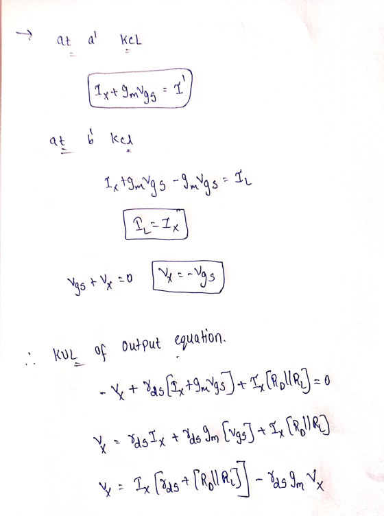
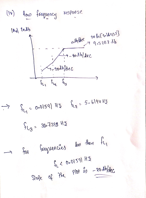
Figure 1 shows an amplifier application using a JFET. Given that Vasq=-2.48 V. IDQ = 2.07...
Figure 1 shows an amplifier application using a JFET. Given that VGSQ = -2.48 V, Ipo...
 Figure 1 shows an amplifier application using a JFET. Given that VGSQ = -2.48 V, Ipo = 2.07 mA and yes = 0.1 ms. i) Determine the voltage gain at mid-range frequency, Avimid). ii) Determine fia, fic and fis for the network. iii) Determine which value contributes to the low frequency response for the network. iv) Plot the asymptotes for low frequency response of the network. Use the semi-log graph paper given in APPENDIX II for your answer. v) Plot...
Figure 1 shows an amplifier application using a JFET. Given that Vaso = -0.87 V, IpQ...
 Figure 1 shows an amplifier application using a JFET. Given that Vaso = -0.87 V, IpQ = 9.82 mA and you = 5 MS. i) Determine the voltage gain at mid-range frequency, Aumid). 1) Determine the fofuc and fis for the network ii) Determine which f. contributes to the low frequency response for the system. [20 Marks) Other Capacitors: 9 Vo 28 V Cos = 6 pF Cos = 1 pF Con = 4 pF R, - 4 MO Cwi...
help me please Question: 20 V Cwi Cw 220 k12 4 pF C - 8 pF...
 help me please
Question: 20 V Cwi Cw 220 k12 4 pF C - 8 pF 6 pF Ces = 12 pF Ca - 3pF 3.9 k2 6.8 uF HE loss = 10 mA Vp = -6 V 1.5 k92 WE 1uF + 5.6 ks2 68 k12 w 2.2 ks 10uF Determine fio, fic and fus with ra = 100 k2 Identify the actual cut off frequency and draw the low-frequency response of the network using Multisim. Discuss your results.
help me please
Question: 20 V Cwi Cw 220 k12 4 pF C - 8 pF 6 pF Ces = 12 pF Ca - 3pF 3.9 k2 6.8 uF HE loss = 10 mA Vp = -6 V 1.5 k92 WE 1uF + 5.6 ks2 68 k12 w 2.2 ks 10uF Determine fio, fic and fus with ra = 100 k2 Identify the actual cut off frequency and draw the low-frequency response of the network using Multisim. Discuss your results.
Determine the lower and upper cutoff frequency for the network. Sketch the frequency response using bode plot 2. A self-biased n-channel JFET Amplifier with C1(input)-0.01uF C2(bypass)-2uF C3(...
 Determine the lower and upper cutoff frequency for the network.
Sketch the frequency response using bode plot
2. A self-biased n-channel JFET Amplifier with C1(input)-0.01uF C2(bypass)-2uF C3(output)-0.5uF VDD 20V Rsig- 10kQ RG-1M Ω RD-4.7k Q IDSS-8mA VGS(off-AV Cgd-2pF Cgs-4pF Cds-0.5pF Cwo-6pF RL-2.2k Ω Rc rQi=120 0.47uF R, 04uF 0.82Ω R: 2. A self-biased n-channel JFET Amplifier with C1 (input)=001uF C2bypass)-2uF C3(output):0.5UF VDD-20V Rsige 10kΩ RG-1M Ω RD-4.7k Ω IDSS-BmA VGS(off)-4V Cgd-2pF Cds-0.5pF Cwi-5pF RL-2.2k Ω
2. A self-biased n-channel JFET...
Determine the lower and upper cutoff frequency for the network.
Sketch the frequency response using bode plot
2. A self-biased n-channel JFET Amplifier with C1(input)-0.01uF C2(bypass)-2uF C3(output)-0.5uF VDD 20V Rsig- 10kQ RG-1M Ω RD-4.7k Q IDSS-8mA VGS(off-AV Cgd-2pF Cgs-4pF Cds-0.5pF Cwo-6pF RL-2.2k Ω Rc rQi=120 0.47uF R, 04uF 0.82Ω R: 2. A self-biased n-channel JFET Amplifier with C1 (input)=001uF C2bypass)-2uF C3(output):0.5UF VDD-20V Rsige 10kΩ RG-1M Ω RD-4.7k Ω IDSS-BmA VGS(off)-4V Cgd-2pF Cds-0.5pF Cwi-5pF RL-2.2k Ω
2. A self-biased n-channel JFET...
1. Determine fio, fic and fus with ra = 100 ks Identify the actual cut off...
 1. Determine fio, fic and fus with ra = 100 ks Identify the actual cut off frequency. 2. draw the low-frequency response of the network using Multisim. 3. Discuss your results. 20 V Cw Cw 4 pF Cod = 8 pF = 6 pF C = 12 pF Com = 3pF 3.9 k92 220 kΩ 6.8 uF HE loss = 10 mA Vp = -6 V 1.5 k92 WE 1μF + 5.6 k 2 68 k22 21 2.2 k92 10uF...
1. Design the common source amplifier shown in Figure 1 with Ip- 1 mA and Vo 5 V Determine V2 and Ri. The MOSFET characteristics are V-50 V, k-0.093 A/V, gate-to- drain capacitance, Cd 40 pF,...
 1. Design the common source amplifier shown in Figure 1 with Ip- 1 mA and Vo 5 V Determine V2 and Ri. The MOSFET characteristics are V-50 V, k-0.093 A/V, gate-to- drain capacitance, Cd 40 pF, and Vi 1.1 V. (For PSpice simulations, use parameters: VTO. 1.1 LAMBDA-002 KP-0.093 CGDO-4E-7 w=100u L-I00u for the 2N7000 MOSFET.) a. Determine the gain and gm of the circuit b. Determine the low-frequency (high-pass response) poles of the common-source amplifier due to the coupling...
A common source amplifier circuit based on a single n-channel MOSFET is shown in Figure 4b. Assume that the transconductance gm-60 mS (equivalent to mA/ V) and drain source resistance, os,...
 A common source amplifier circuit based on a single n-channel MOSFET is shown in Figure 4b. Assume that the transconductance gm-60 mS (equivalent to mA/ V) and drain source resistance, os, is so large it may be neglected. 0) Calculate the open circuit voltage gain Av Yout/ Vis. i) The amplifier has a load of 10 k2. Determine the current gain Va. = 12 V 150k 4k3 Vout Vin 200k GND = 0 V Figure 4b a) State the name...
 Figure 1 shows an amplifier application using a JFET. Given that VGSQ = -2.48 V, Ipo = 2.07 mA and yes = 0.1 ms. i) Determine the voltage gain at mid-range frequency, Avimid). ii) Determine fia, fic and fis for the network. iii) Determine which value contributes to the low frequency response for the network. iv) Plot the asymptotes for low frequency response of the network. Use the semi-log graph paper given in APPENDIX II for your answer. v) Plot...
 Figure 1 shows an amplifier application using a JFET. Given that Vaso = -0.87 V, IpQ = 9.82 mA and you = 5 MS. i) Determine the voltage gain at mid-range frequency, Aumid). 1) Determine the fofuc and fis for the network ii) Determine which f. contributes to the low frequency response for the system. [20 Marks) Other Capacitors: 9 Vo 28 V Cos = 6 pF Cos = 1 pF Con = 4 pF R, - 4 MO Cwi...
 help me please
Question: 20 V Cwi Cw 220 k12 4 pF C - 8 pF 6 pF Ces = 12 pF Ca - 3pF 3.9 k2 6.8 uF HE loss = 10 mA Vp = -6 V 1.5 k92 WE 1uF + 5.6 ks2 68 k12 w 2.2 ks 10uF Determine fio, fic and fus with ra = 100 k2 Identify the actual cut off frequency and draw the low-frequency response of the network using Multisim. Discuss your results.
help me please
Question: 20 V Cwi Cw 220 k12 4 pF C - 8 pF 6 pF Ces = 12 pF Ca - 3pF 3.9 k2 6.8 uF HE loss = 10 mA Vp = -6 V 1.5 k92 WE 1uF + 5.6 ks2 68 k12 w 2.2 ks 10uF Determine fio, fic and fus with ra = 100 k2 Identify the actual cut off frequency and draw the low-frequency response of the network using Multisim. Discuss your results.
 Determine the lower and upper cutoff frequency for the network.
Sketch the frequency response using bode plot
2. A self-biased n-channel JFET Amplifier with C1(input)-0.01uF C2(bypass)-2uF C3(output)-0.5uF VDD 20V Rsig- 10kQ RG-1M Ω RD-4.7k Q IDSS-8mA VGS(off-AV Cgd-2pF Cgs-4pF Cds-0.5pF Cwo-6pF RL-2.2k Ω Rc rQi=120 0.47uF R, 04uF 0.82Ω R: 2. A self-biased n-channel JFET Amplifier with C1 (input)=001uF C2bypass)-2uF C3(output):0.5UF VDD-20V Rsige 10kΩ RG-1M Ω RD-4.7k Ω IDSS-BmA VGS(off)-4V Cgd-2pF Cds-0.5pF Cwi-5pF RL-2.2k Ω
2. A self-biased n-channel JFET...
Determine the lower and upper cutoff frequency for the network.
Sketch the frequency response using bode plot
2. A self-biased n-channel JFET Amplifier with C1(input)-0.01uF C2(bypass)-2uF C3(output)-0.5uF VDD 20V Rsig- 10kQ RG-1M Ω RD-4.7k Q IDSS-8mA VGS(off-AV Cgd-2pF Cgs-4pF Cds-0.5pF Cwo-6pF RL-2.2k Ω Rc rQi=120 0.47uF R, 04uF 0.82Ω R: 2. A self-biased n-channel JFET Amplifier with C1 (input)=001uF C2bypass)-2uF C3(output):0.5UF VDD-20V Rsige 10kΩ RG-1M Ω RD-4.7k Ω IDSS-BmA VGS(off)-4V Cgd-2pF Cds-0.5pF Cwi-5pF RL-2.2k Ω
2. A self-biased n-channel JFET...
 1. Determine fio, fic and fus with ra = 100 ks Identify the actual cut off frequency. 2. draw the low-frequency response of the network using Multisim. 3. Discuss your results. 20 V Cw Cw 4 pF Cod = 8 pF = 6 pF C = 12 pF Com = 3pF 3.9 k92 220 kΩ 6.8 uF HE loss = 10 mA Vp = -6 V 1.5 k92 WE 1μF + 5.6 k 2 68 k22 21 2.2 k92 10uF...
 1. Design the common source amplifier shown in Figure 1 with Ip- 1 mA and Vo 5 V Determine V2 and Ri. The MOSFET characteristics are V-50 V, k-0.093 A/V, gate-to- drain capacitance, Cd 40 pF, and Vi 1.1 V. (For PSpice simulations, use parameters: VTO. 1.1 LAMBDA-002 KP-0.093 CGDO-4E-7 w=100u L-I00u for the 2N7000 MOSFET.) a. Determine the gain and gm of the circuit b. Determine the low-frequency (high-pass response) poles of the common-source amplifier due to the coupling...
 A common source amplifier circuit based on a single n-channel MOSFET is shown in Figure 4b. Assume that the transconductance gm-60 mS (equivalent to mA/ V) and drain source resistance, os, is so large it may be neglected. 0) Calculate the open circuit voltage gain Av Yout/ Vis. i) The amplifier has a load of 10 k2. Determine the current gain Va. = 12 V 150k 4k3 Vout Vin 200k GND = 0 V Figure 4b a) State the name...
Most questions answered within 3 hours.
-
Six years of quarterly data of a seasonally adjusted series are
used to estimate a linear...
asked 5 minutes ago -
Which of the following is not an ecological model used
to foster behavior change?
PRECEDE-PROCEED Model...
asked 8 minutes ago -
On the Apollo 14 mission to the moon, astronaut Alan Shepard hit
a golf ball with...
asked 4 minutes ago -
What are John’s potential claims if he is terminated
this week?
John is a 54-year-old man...
asked 18 minutes ago -
A (8.5) cm tall object is placed at a distance of (14.2) cm from
a convex...
asked 26 minutes ago -
(2) For the following questions, consider a data set that
exhibits a normal distribution. Report the...
asked 27 minutes ago -
What exactly is an information system? How does it work" What
are its people organization,
...
asked 29 minutes ago -
The Food Marketing Institute shows that 17% of households spend
more than $100 per week on...
asked 38 minutes ago -
Go to NCBI BLAST search web page
1st search: GEKDLRRAKDINQEVYNF
2nd search: PTSQRLQLLEPFDK
3rd search: GEKDLRRAKDINQEVYNF...
asked 42 minutes ago -
Explain how each of the following three conditions could be a
red flag for a register...
asked 46 minutes ago -
In a two-way factorial ANOVA, the final F-ratio for
factor AxB is determined by dividing _____...
asked 1 hour ago -
Show your solutions for answer.
4. An aqueous solution contains 9.21 g of
K4Fe(CN)6 in a...
asked 47 minutes ago