PART B: OPAMP as a non-inverting
amplifier
a) Implement the following circuit using the LM741
and energize the integrated circuit 741 with + 15v and -15v. In
addition, feed the circuit with a 1 Vpp and 1KHz sinusoidal signal.
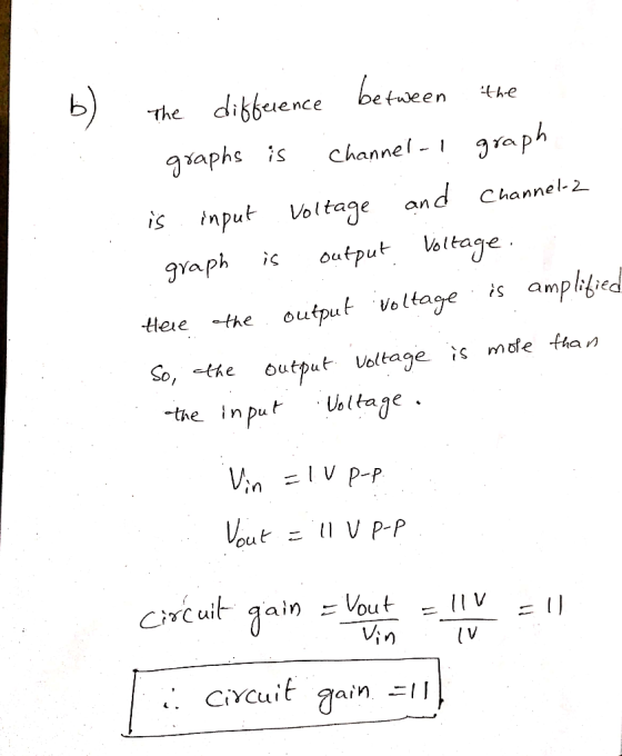
Values: R2 = 10kΩ, R1 = 1KΩ

b) Obtain the graph of the output voltage and the input voltage. Explain the differences between the graphs and determine the circuit gain.

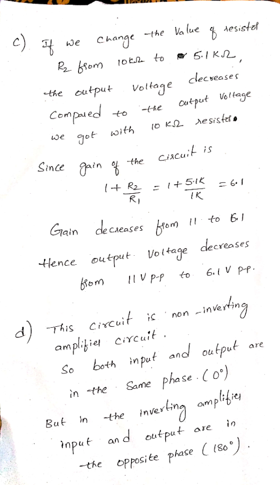
c) Change the R2 resistor with a 5.1k Ω resistor. Obtain again the graph of output voltage and input voltage. What happens to the output voltage of the circuit? Explain

d) What differences did you observe with respect to the inverting amplifier implemented in the previous circuit?
Homework Answers
Answered the question below.
If you have any doubt ask in the comment section.
Please rate if you like my answer.
b) Output and input graphs when R2 = 10K

C) Output and input graphs when R2 = 5.1K

Add Answer to:
PART B: OPAMP as a non-inverting
amplifier
a) Implement the following circuit using the LM741
and...
5,6,7 5- Theoretical Part: For the same above circuit (Part B), First, change Rx to 2.2K....
 5,6,7
5- Theoretical Part: For the same above circuit (Part B), First, change Rx to 2.2K. What is the maximum peak input voltage before Vout just saturates? Assume the dc input is still at 1.5V (unchanged) (Assume Vsat = 10Volts ) Vin(pk) maximum = ......................-Volts 6- Verify the theoretical result in 5 by slowly varying the amplitude of the input signal until Vout just saturates (about to saturate). What is the corresponding Vin(pk)? Vin(pk) maximum = ................. Volts 7. If...
5,6,7
5- Theoretical Part: For the same above circuit (Part B), First, change Rx to 2.2K. What is the maximum peak input voltage before Vout just saturates? Assume the dc input is still at 1.5V (unchanged) (Assume Vsat = 10Volts ) Vin(pk) maximum = ......................-Volts 6- Verify the theoretical result in 5 by slowly varying the amplitude of the input signal until Vout just saturates (about to saturate). What is the corresponding Vin(pk)? Vin(pk) maximum = ................. Volts 7. If...
2. Consider this non-inverting op-amp amplifier This non-inverting amplifier circuit uses an operational amplifier as a...
 2. Consider this non-inverting op-amp amplifier This non-inverting amplifier circuit uses an operational amplifier as a building block. Do around. The op-amp's gain is a "little a"), but the overall amplifier's gain is A Cbig A. Derive the value of the output voltage, ve, as a function of the input voltage not confuse the non-inverting amplifier with the operational amplifier that it is built a. and the op-amp's gain a. What is the overall amplifier's gain Avo/v? (20pts) b. We...
Problem # 3 For the summing opamp circuit, assume that the opamp is powered with +15V and-15V. Th...
 Problem # 3 For the summing opamp circuit, assume that the opamp is powered with +15V and-15V. The input voltages are VI and V2 and the output voltage is Vout. Rf 15 V U1 R1 R2 Vout 741 V2 (A -15 V 1. Find the relation between the output Vout and the inputs VI and V2 2. Assume that RI-2kS2, R2-3 ㏀ and Rf-6kS2, Vin is a sinewave with viinpp-2V, V2DC- IV, plot Vin() and Vout(0) 3. Assume that you...
Part I: Inverting Amplifier Procedure: 1. Build the circuit model for inverting amplifier in PSpice with...
 Part I: Inverting Amplifier Procedure: 1. Build the circuit model for inverting amplifier in PSpice with the following parameters: Ri = 5 k 2, R2 = 20 ks2, V+ = 10 V, V-=-10 V. 2. Hand calculates the theoretical closed loop gain Vout/Vin of the circuit model. 3. Generate a triangular waveform for Vin with the amplitude of 1 V and the period of 1 ms. 4. Run simulation. a. Set circuit model parameters. i.e., for voltage source: click VPWL...
2. Construct the non-inverting amplifier circuit below. Then, obtain input-output transfer function for R1=1K and R2=2.2K,...
 2. Construct the non-inverting amplifier circuit below. Then, obtain input-output transfer function for R1=1K and R2=2.2K, E= 9V. Use a variable de voltage (5V de source and a variable 1k potentiometer) source as the input and measure the output voltage for different inputs. Draw the input-output transfer function from the measured input-output voltages. Proteus Table Vin Vout Measured Table Vin Vout Q2) Determine the voltage gain VO / Vin of the non-inverting amplifier. What is the output voltage range over...
Inverting Amplifier Figure 4.2 shows the fundamental configuration of Op-Amp in which it is used as...
 Inverting Amplifier Figure 4.2 shows the fundamental configuration of Op-Amp in which it is used as an inverting amplifier. In this configuration the ratio, R2/R1 completely controls the effective gain of the amplifier and it can be verified that the output voltage is equal to Vo = - (R2/R1)Vin R2 100K Q-10V R1 Vinow 20K 1 2 7 V Vo 3 -10v Figure 4.2 Part 1 - Inverting Amp: Procedure 1. Construct the circuit of figure 4.2 using Op-Amp IC...
EE 213: Linear Circuit Analysis Final Project Strain Gauge Amplifier A Force sensing strain gauge is...
 EE 213: Linear Circuit Analysis Final Project Strain Gauge Amplifier A Force sensing strain gauge is rate at 2225 N. It is supplied by 11 V source and provides 3mV/V at the rated force. This means that the output of the staring gauge will be 33 mV if the force was 2225 N and -33 mV if the force was -2225N. Design an operation amplifier circuit to convert this voltage range from -33-33 mV to 0-3.3V. One terminal of the...
(a) A voltage divider bypassed common-source (CS) FET amplifier biasing circuit with load R, is commonly...
 (a) A voltage divider bypassed common-source (CS) FET amplifier biasing circuit with load R, is commonly used in electronic circuit. (1) Design the circuit of a voltage divider bypassed common-source FET amplifier biasing circuit with load Ru. [4 marks) (ii) By referring to Q4(a)(i), design a bypassed common-source FET amplifier with biasing voltage-divider to meet the given specifications below: Supply voltage, Vcc = 12 V; Voltage gain, Ay = -10; Output load Ru = 10 kV2; input impedance Zi =...
please show steps, and solve asap BEE 433 Electronic Circuit Design Problem Set #1 Due date:...
 please show steps, and solve asap
BEE 433 Electronic Circuit Design Problem Set #1 Due date: Answer the following problems and Circle the answers. 1.1 (Fig. 1.1 from the textbook) In the voltage amplifier circuit of Fig. 1.1, let vs = 100 mV, Rs = 100 k 52, Vi = 75 mV, RL = 10 S2, and vo = 2 V. If connecting a 30-S2 resistance in parallel with RL drops vo to 1.8 V, find Ri, A., and R....
please show steps, and solve asap
BEE 433 Electronic Circuit Design Problem Set #1 Due date: Answer the following problems and Circle the answers. 1.1 (Fig. 1.1 from the textbook) In the voltage amplifier circuit of Fig. 1.1, let vs = 100 mV, Rs = 100 k 52, Vi = 75 mV, RL = 10 S2, and vo = 2 V. If connecting a 30-S2 resistance in parallel with RL drops vo to 1.8 V, find Ri, A., and R....
Laboratory 1: operation amplifier characteristics A. Objectives: 1. To study the basic characteri...
 thanks
Laboratory 1: operation amplifier characteristics A. Objectives: 1. To study the basic characteristics of an operational amplifier 2. To study the bias circuit of an operational amplifier B. Apparatus: 1. DC Power supply 2. Experimental board and corresponding components 3. Electronic calculator (prepared by students) 4. Digital camera (prepared by students for photo taking of the experimental results) 5. Laptop computer with the software PicoScope 6 and Microsoft Word installed. 6. PicoScope PC Oscilloscope and its accessories. 7. Multimeter...
thanks
Laboratory 1: operation amplifier characteristics A. Objectives: 1. To study the basic characteristics of an operational amplifier 2. To study the bias circuit of an operational amplifier B. Apparatus: 1. DC Power supply 2. Experimental board and corresponding components 3. Electronic calculator (prepared by students) 4. Digital camera (prepared by students for photo taking of the experimental results) 5. Laptop computer with the software PicoScope 6 and Microsoft Word installed. 6. PicoScope PC Oscilloscope and its accessories. 7. Multimeter...
 5,6,7
5- Theoretical Part: For the same above circuit (Part B), First, change Rx to 2.2K. What is the maximum peak input voltage before Vout just saturates? Assume the dc input is still at 1.5V (unchanged) (Assume Vsat = 10Volts ) Vin(pk) maximum = ......................-Volts 6- Verify the theoretical result in 5 by slowly varying the amplitude of the input signal until Vout just saturates (about to saturate). What is the corresponding Vin(pk)? Vin(pk) maximum = ................. Volts 7. If...
5,6,7
5- Theoretical Part: For the same above circuit (Part B), First, change Rx to 2.2K. What is the maximum peak input voltage before Vout just saturates? Assume the dc input is still at 1.5V (unchanged) (Assume Vsat = 10Volts ) Vin(pk) maximum = ......................-Volts 6- Verify the theoretical result in 5 by slowly varying the amplitude of the input signal until Vout just saturates (about to saturate). What is the corresponding Vin(pk)? Vin(pk) maximum = ................. Volts 7. If...
 2. Consider this non-inverting op-amp amplifier This non-inverting amplifier circuit uses an operational amplifier as a building block. Do around. The op-amp's gain is a "little a"), but the overall amplifier's gain is A Cbig A. Derive the value of the output voltage, ve, as a function of the input voltage not confuse the non-inverting amplifier with the operational amplifier that it is built a. and the op-amp's gain a. What is the overall amplifier's gain Avo/v? (20pts) b. We...
 Problem # 3 For the summing opamp circuit, assume that the opamp is powered with +15V and-15V. The input voltages are VI and V2 and the output voltage is Vout. Rf 15 V U1 R1 R2 Vout 741 V2 (A -15 V 1. Find the relation between the output Vout and the inputs VI and V2 2. Assume that RI-2kS2, R2-3 ㏀ and Rf-6kS2, Vin is a sinewave with viinpp-2V, V2DC- IV, plot Vin() and Vout(0) 3. Assume that you...
 Part I: Inverting Amplifier Procedure: 1. Build the circuit model for inverting amplifier in PSpice with the following parameters: Ri = 5 k 2, R2 = 20 ks2, V+ = 10 V, V-=-10 V. 2. Hand calculates the theoretical closed loop gain Vout/Vin of the circuit model. 3. Generate a triangular waveform for Vin with the amplitude of 1 V and the period of 1 ms. 4. Run simulation. a. Set circuit model parameters. i.e., for voltage source: click VPWL...
 2. Construct the non-inverting amplifier circuit below. Then, obtain input-output transfer function for R1=1K and R2=2.2K, E= 9V. Use a variable de voltage (5V de source and a variable 1k potentiometer) source as the input and measure the output voltage for different inputs. Draw the input-output transfer function from the measured input-output voltages. Proteus Table Vin Vout Measured Table Vin Vout Q2) Determine the voltage gain VO / Vin of the non-inverting amplifier. What is the output voltage range over...
 Inverting Amplifier Figure 4.2 shows the fundamental configuration of Op-Amp in which it is used as an inverting amplifier. In this configuration the ratio, R2/R1 completely controls the effective gain of the amplifier and it can be verified that the output voltage is equal to Vo = - (R2/R1)Vin R2 100K Q-10V R1 Vinow 20K 1 2 7 V Vo 3 -10v Figure 4.2 Part 1 - Inverting Amp: Procedure 1. Construct the circuit of figure 4.2 using Op-Amp IC...
 EE 213: Linear Circuit Analysis Final Project Strain Gauge Amplifier A Force sensing strain gauge is rate at 2225 N. It is supplied by 11 V source and provides 3mV/V at the rated force. This means that the output of the staring gauge will be 33 mV if the force was 2225 N and -33 mV if the force was -2225N. Design an operation amplifier circuit to convert this voltage range from -33-33 mV to 0-3.3V. One terminal of the...
 (a) A voltage divider bypassed common-source (CS) FET amplifier biasing circuit with load R, is commonly used in electronic circuit. (1) Design the circuit of a voltage divider bypassed common-source FET amplifier biasing circuit with load Ru. [4 marks) (ii) By referring to Q4(a)(i), design a bypassed common-source FET amplifier with biasing voltage-divider to meet the given specifications below: Supply voltage, Vcc = 12 V; Voltage gain, Ay = -10; Output load Ru = 10 kV2; input impedance Zi =...
 please show steps, and solve asap
BEE 433 Electronic Circuit Design Problem Set #1 Due date: Answer the following problems and Circle the answers. 1.1 (Fig. 1.1 from the textbook) In the voltage amplifier circuit of Fig. 1.1, let vs = 100 mV, Rs = 100 k 52, Vi = 75 mV, RL = 10 S2, and vo = 2 V. If connecting a 30-S2 resistance in parallel with RL drops vo to 1.8 V, find Ri, A., and R....
please show steps, and solve asap
BEE 433 Electronic Circuit Design Problem Set #1 Due date: Answer the following problems and Circle the answers. 1.1 (Fig. 1.1 from the textbook) In the voltage amplifier circuit of Fig. 1.1, let vs = 100 mV, Rs = 100 k 52, Vi = 75 mV, RL = 10 S2, and vo = 2 V. If connecting a 30-S2 resistance in parallel with RL drops vo to 1.8 V, find Ri, A., and R....
 thanks
Laboratory 1: operation amplifier characteristics A. Objectives: 1. To study the basic characteristics of an operational amplifier 2. To study the bias circuit of an operational amplifier B. Apparatus: 1. DC Power supply 2. Experimental board and corresponding components 3. Electronic calculator (prepared by students) 4. Digital camera (prepared by students for photo taking of the experimental results) 5. Laptop computer with the software PicoScope 6 and Microsoft Word installed. 6. PicoScope PC Oscilloscope and its accessories. 7. Multimeter...
thanks
Laboratory 1: operation amplifier characteristics A. Objectives: 1. To study the basic characteristics of an operational amplifier 2. To study the bias circuit of an operational amplifier B. Apparatus: 1. DC Power supply 2. Experimental board and corresponding components 3. Electronic calculator (prepared by students) 4. Digital camera (prepared by students for photo taking of the experimental results) 5. Laptop computer with the software PicoScope 6 and Microsoft Word installed. 6. PicoScope PC Oscilloscope and its accessories. 7. Multimeter...
Most questions answered within 3 hours.
-
Your system is rejecting the question am asking which is
preceded by a case study. It...
asked 1 minute from now -
A member of the volleyball team spikes the ball. During this
process, she changes the velocity...
asked 2 minutes ago -
Are adult gamers less likely to use a gaming console (Xbox,
PlayStation, Wii, etc...) than teen...
asked 55 minutes ago -
The University of
Texas recently reported that 43% of college students aged 18-24
would spend their...
asked 1 hour ago -
The length of stay at a specific emergency department in
Phoenix, Arizona, in 2009 had a...
asked 22 minutes ago -
. Please give the mechanism for this type of problem. Step by
Step
The toxin that...
asked 25 minutes ago -
If you have a 1M stock solution and you want to dilute 1 :10
with water,...
asked 27 minutes ago -
In a load instruction, the effective address is obtained by
A) Retriving the address from a...
asked 27 minutes ago -
Use the following information to answer this question.
Windswept, Inc. 2017 Income Statement ($ in millions)...
asked 28 minutes ago -
A mutual fund salesperson has arranged to call on four people
tomorrow. Based on past experience...
asked 1 hour ago -
Let the RV Y has the pdf
f ( y ) = 6 y ( 1...
asked 1 hour ago -
Question 12
Where should a copy of a private key should be placed so it is...
asked 30 minutes ago