
Homework Answers

Add Answer to:
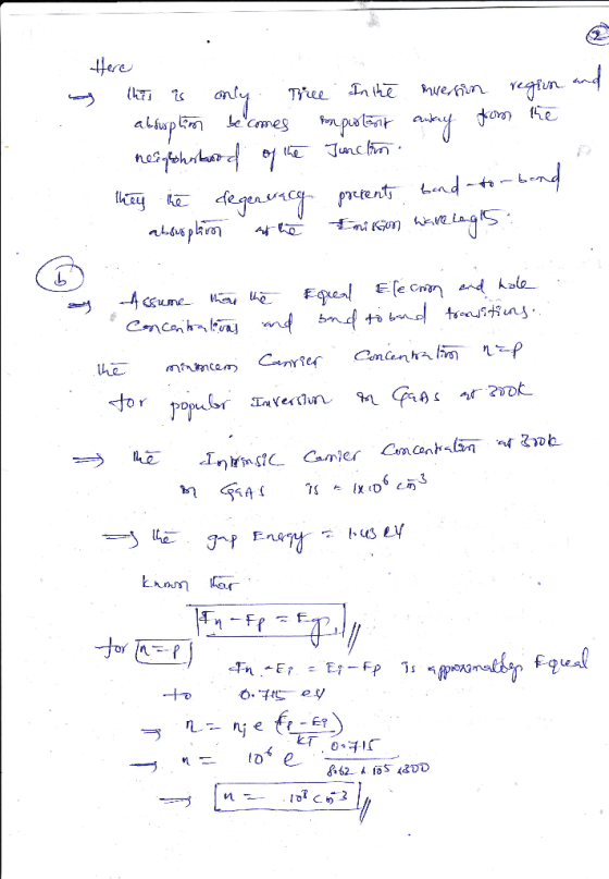
GaAs laser (a) The degenerate occupation of the conduction and valence bands with electrons and holes...
Please help me 1. In degenerate p-type silicon, a. The Fermi energy is above the valence...
 Please help me
1. In degenerate p-type silicon, a. The Fermi energy is above the valence energy and below the intrinsic Fermi energy b. The Fermi energy is below the valence energy c. The Fermi energy is above the conduction energy d. The Fermi energy is below the conduction energy and above the intrinsic Fermi energy 2. A semiconductor has No 5X 1010 cm3 and N-2X 1018 cm2. It is a. b. C. d. N-type and electrons are the majority...
Please help me
1. In degenerate p-type silicon, a. The Fermi energy is above the valence energy and below the intrinsic Fermi energy b. The Fermi energy is below the valence energy c. The Fermi energy is above the conduction energy d. The Fermi energy is below the conduction energy and above the intrinsic Fermi energy 2. A semiconductor has No 5X 1010 cm3 and N-2X 1018 cm2. It is a. b. C. d. N-type and electrons are the majority...
e Calculate the position of EF with respect to E. 5. Explain why holes are found...
 e Calculate the position of EF with respect to E. 5. Explain why holes are found wny holes are found near the top of the valence band, whereas conduction electrons are found at the bottom of the conduction band. O. Using the Figure 3-17 in your text (also attached), fill in the following table: Semiconductor 300°K 400°K 500°K Ge GaAs For Ge at 500°K and Si at 400°K, show on the attached graph how you determined the value you put...
You have an intrinsic semiconductor. (a) When temperature T = 0[K], obtain the density of electrons...
You have an intrinsic semiconductor. (a) When temperature T = 0[K], obtain the density of electrons n in the conduction band and that of holes p in the valence band; (b) When T = 300[K], obtain the mathematical relationship between n and p (e.g., n=p, n>p, or n<p); (c) When T = 300[K], obtain the mathematical relationship between the np product and the intrinsic carrier concentration ni.
(2) In a semiconductor with an energy gap Eg between the valence and the conduction bands we can take Ef (the Fermi ene...
 (2) In a semiconductor with an energy gap Eg between the valence and the conduction bands we can take Ef (the Fermi energy) to be halfway between the bands (see figure below): Conduction band Energy gap Eg Valence band Semiconductor a. Show that for a typical semiconductor or insulator at room temperature the Fermi- Dirac factor is approximately equal to exp(-E 2kBT). (Typical Eg for semi-conductors ranges from about 0.5eV to 6eV at T-293K.) b. In heavily doped n-type silicon,...
Please explain part b in details thx! Question 2 At 300 K, the bandgap of GaP is 2.26 eV and the effective density of states at the conduction and valence band edge are 1.8 x 1019 cm23 and 1.9 x 10¹⁹...
 Please explain part b in details thx!
Question 2 At 300 K, the bandgap of GaP is 2.26 eV and the effective density of states at the conduction and valence band edge are 1.8 x 1019 cm23 and 1.9 x 1019 cm3, respectively. (a) Calculate the intrinsic concentration of GaP at 300K (7 marks) Calculate the GaP effective mass of holes at 300K. (b) (8 marks) (c The GaP sample is now doped with donor concentration of 1021 cm3 with...
Please explain part b in details thx!
Question 2 At 300 K, the bandgap of GaP is 2.26 eV and the effective density of states at the conduction and valence band edge are 1.8 x 1019 cm23 and 1.9 x 1019 cm3, respectively. (a) Calculate the intrinsic concentration of GaP at 300K (7 marks) Calculate the GaP effective mass of holes at 300K. (b) (8 marks) (c The GaP sample is now doped with donor concentration of 1021 cm3 with...
Special Problem (20 pts) Consider an undoped AljGa7As/GaAs/ Al3Ga7As quantum well (QW) of width W...
 Special Problem (20 pts) Consider an undoped AljGa7As/GaAs/ Al3Ga7As quantum well (QW) of width W-15 nm. (a) Due the quantum mechanical confinement in the quantum well, the lowest energy states of in the conduction band is no longer the conduction band edge, but the CB edge plus the confined state energy (particle in the box problem), where the confinement energy relative to the CB edge is given by the solutions for infinite barriers where n-1,2,.is the quantum number, n-1 is...
EENG 245 Physical electronics HW 1 1) The NaCl crystal is cubic, and can be described...
 EENG 245 Physical electronics HW 1 1) The NaCl crystal is cubic, and can be described as follows. Na atoms sit at the corners and faces of a cube, and Cl atoms sit in between two Na atoms. This means that a Clatom is found half-way along each of the cube edges, and there is a Cl in the center of the cube. (We could also have described the lattice by interchanging Na and Cl in the description above.) Another...
 Please help me
1. In degenerate p-type silicon, a. The Fermi energy is above the valence energy and below the intrinsic Fermi energy b. The Fermi energy is below the valence energy c. The Fermi energy is above the conduction energy d. The Fermi energy is below the conduction energy and above the intrinsic Fermi energy 2. A semiconductor has No 5X 1010 cm3 and N-2X 1018 cm2. It is a. b. C. d. N-type and electrons are the majority...
Please help me
1. In degenerate p-type silicon, a. The Fermi energy is above the valence energy and below the intrinsic Fermi energy b. The Fermi energy is below the valence energy c. The Fermi energy is above the conduction energy d. The Fermi energy is below the conduction energy and above the intrinsic Fermi energy 2. A semiconductor has No 5X 1010 cm3 and N-2X 1018 cm2. It is a. b. C. d. N-type and electrons are the majority...
 e Calculate the position of EF with respect to E. 5. Explain why holes are found wny holes are found near the top of the valence band, whereas conduction electrons are found at the bottom of the conduction band. O. Using the Figure 3-17 in your text (also attached), fill in the following table: Semiconductor 300°K 400°K 500°K Ge GaAs For Ge at 500°K and Si at 400°K, show on the attached graph how you determined the value you put...
 (2) In a semiconductor with an energy gap Eg between the valence and the conduction bands we can take Ef (the Fermi energy) to be halfway between the bands (see figure below): Conduction band Energy gap Eg Valence band Semiconductor a. Show that for a typical semiconductor or insulator at room temperature the Fermi- Dirac factor is approximately equal to exp(-E 2kBT). (Typical Eg for semi-conductors ranges from about 0.5eV to 6eV at T-293K.) b. In heavily doped n-type silicon,...
 Please explain part b in details thx!
Question 2 At 300 K, the bandgap of GaP is 2.26 eV and the effective density of states at the conduction and valence band edge are 1.8 x 1019 cm23 and 1.9 x 1019 cm3, respectively. (a) Calculate the intrinsic concentration of GaP at 300K (7 marks) Calculate the GaP effective mass of holes at 300K. (b) (8 marks) (c The GaP sample is now doped with donor concentration of 1021 cm3 with...
Please explain part b in details thx!
Question 2 At 300 K, the bandgap of GaP is 2.26 eV and the effective density of states at the conduction and valence band edge are 1.8 x 1019 cm23 and 1.9 x 1019 cm3, respectively. (a) Calculate the intrinsic concentration of GaP at 300K (7 marks) Calculate the GaP effective mass of holes at 300K. (b) (8 marks) (c The GaP sample is now doped with donor concentration of 1021 cm3 with...
 Special Problem (20 pts) Consider an undoped AljGa7As/GaAs/ Al3Ga7As quantum well (QW) of width W-15 nm. (a) Due the quantum mechanical confinement in the quantum well, the lowest energy states of in the conduction band is no longer the conduction band edge, but the CB edge plus the confined state energy (particle in the box problem), where the confinement energy relative to the CB edge is given by the solutions for infinite barriers where n-1,2,.is the quantum number, n-1 is...
 EENG 245 Physical electronics HW 1 1) The NaCl crystal is cubic, and can be described as follows. Na atoms sit at the corners and faces of a cube, and Cl atoms sit in between two Na atoms. This means that a Clatom is found half-way along each of the cube edges, and there is a Cl in the center of the cube. (We could also have described the lattice by interchanging Na and Cl in the description above.) Another...
Most questions answered within 3 hours.
-
You have a 825.3 mL sample of 2.754 M HA (Ka =
4.49⋅10−4). Calculate the pH...
asked 19 seconds from now -
The blues made its way into many kinds of music. Eric Clapton,
The Beatles, and Elvis...
asked 2 hours ago -
8. A wave in a string has a wave function given by: y (x, t) =...
asked 1 hour ago -
If you’re standing at the bottom of a hill and asked to evaluate
it while being...
asked 2 hours ago -
1. Which region has taken the lead in the world of
e-waste handling?
a) European Union...
asked 2 hours ago -
A 8.15- g bullet from a 9-mm pistol has a velocity of 366.0 m/s.
It strikes...
asked 4 hours ago -
The outstanding bonds of Alpha Extracts have a yield to maturity
of 7.4 percent and a...
asked 4 hours ago -
The Problem: The Case of the Harmonizing Vacations
Your CEO is exploring partnering with a European...
asked 5 hours ago -
A chemical equation is balanced by adding coefficients in front
of some formulas so that the...
asked 5 hours ago -
From the literature (reference your sources): What are the
lattice parameters of calcite and aragonite? Why...
asked 6 hours ago -
Your system is rejecting the question am asking which is
preceded by a case study. It...
asked 6 hours ago -
3. On January 2, 2000, Larry creates a trust with himself as
trustee. Larry as trustee...
asked 6 hours ago