
Homework Answers
Add Answer to:
4. Consider the common-emitter amplifier of Figure 5. Draw the dc circuit and find「CQ. Draw the...
4. Consider the common-emitter amplifier of Figure 5. Draw the dc circuit and find ICQ. Draw the dc circuit and find IC...
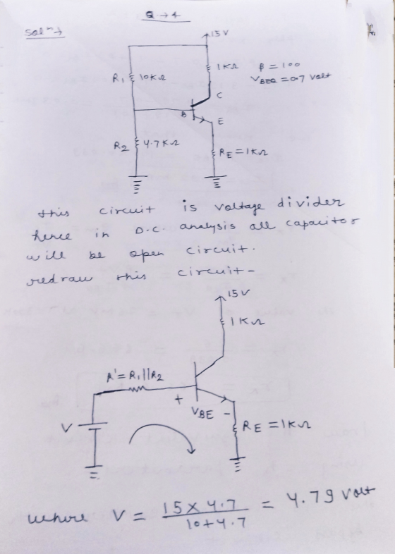
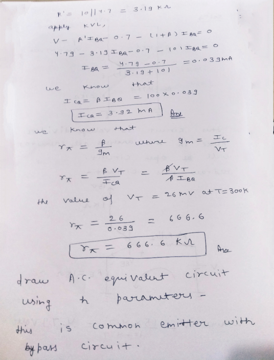
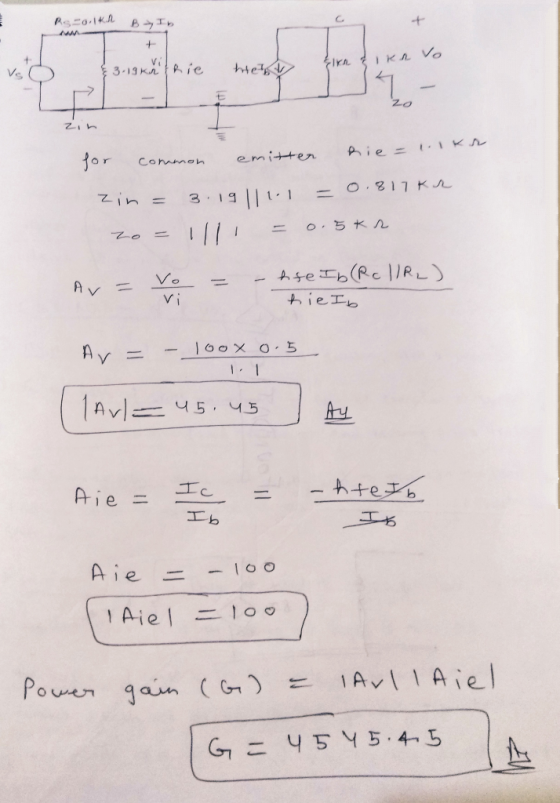
 4. Consider the common-emitter amplifier of Figure 5. Draw the dc circuit and find ICQ. Draw the dc circuit and find ICQ. Find the value of Then, calculate values for Voltage gain Av, Open circuit voltage gain Avoc, input impedance Zin, current gain Ai, power gain G, and out- put impedance Zo. Assume operation in the frequency range for which influence of coupling and bypass capacitors can be ignored +15 V +15 V B 100 100 Ω 47ka Figure 5...
QUESTION 1 Figure Q1 shows a common emitter (CE) and common Base (CB) cascade amplifier circuit....
 QUESTION 1 Figure Q1 shows a common emitter (CE) and common Base (CB) cascade amplifier circuit. Determine the input and output impedance, Z; and Zo, voltage gain, Avi and Av2 and total cascade voltage gain, Ayr and Ays. [25 marks) 2 +8V 1.5 kn 2.2 F 82 k2 3.3 k2 Vo 2.2 uf B = 100 6.8 k12 1 k 2 what B = 100 tuf ZA 5.6 k 2 47012 ZA V. 33 k2 IuF w 10k_2 -2V w...
Avec Úvo SRE L V II. (5pt) Consider the above-right common-collector or emitter-follower BJT amplifier circuit....
 Avec Úvo SRE L V II. (5pt) Consider the above-right common-collector or emitter-follower BJT amplifier circuit. Given: ß= 100, RE = 10 k1, Vcc = 20 V, RB = 5 k1, R1 = 10 kl, and Ry = 2 k1. (a) (1pt) Find the Q-point, i.e. Ibo, Ico, and VCEO; (b) (1pt) draw the small-signal equivalent circuit assuming that the capacitors (C, and Cy) are short circuits for the small signal; (c) (1pt) solve for the voltage gain, Av; (d)...
Font Paragraph Styles 18 Objectives (1) To calculate DC voltages and currents in different sections of...
 Font Paragraph Styles 18 Objectives (1) To calculate DC voltages and currents in different sections of a Common Emitter amplifier. (2) To estimate the voltage gain Av, the input impedance Zin and output impedance Zont of the Common Emitter amplifier. (3) To construct a Common Emitter amplifier circuit on a breadboard. (4) To measure Av, Zin and Zout of the amplifier. Items required 1 Function Generator 1 Variable de power supply 1 Oscilloscope and two scope leads A pair of...
Can I get help with part g through part r, please? Given the following Common-Emitter Amplifier...
 Can I get help with part g through part r, please?
Given the following Common-Emitter Amplifier with Voltage-Divider Bias: The transistor is a Silicon device with B160 (Beta 160) and transistor r.= 30 kn: 20 V 34.7k LAL = Vou 35.10 31.1k LRE $3900 03 - Find the following quantities in parts a through where means Quiescent DC): a) Thevenin Voltage and Thevenin Resistance Re b) Base Current la Collector Current le d) Emitter Current le e) Transistor Collector-Emitter Quiescent...
Can I get help with part g through part r, please?
Given the following Common-Emitter Amplifier with Voltage-Divider Bias: The transistor is a Silicon device with B160 (Beta 160) and transistor r.= 30 kn: 20 V 34.7k LAL = Vou 35.10 31.1k LRE $3900 03 - Find the following quantities in parts a through where means Quiescent DC): a) Thevenin Voltage and Thevenin Resistance Re b) Base Current la Collector Current le d) Emitter Current le e) Transistor Collector-Emitter Quiescent...
Q1. For the cascade amplifier circuit shown in Fig (1): a) What are the functions of the capacitors C, C2 and C3? And w...
 Q1. For the cascade amplifier circuit shown in Fig (1): a) What are the functions of the capacitors C, C2 and C3? And what are the functions of the capacitors Cs and CE? b) What are the functions of the resistors RD and Rc? c) Draw the DC biasing circuits for each stage. d) Find loa, VGsa, VDs and gm for the JFET stage (you may use either mathematical or graphical methods) e) Calculate l, Ic, le and Ve for...
2.A common-emitter circuit with an emitter bypass capacitor is shown in Figure 2(a) and its small-signal...
 2.A common-emitter circuit with an emitter bypass capacitor is shown in Figure 2(a) and its small-signal equivalent is as in Figure 2(b). Let V' = 10 V, V-=-10 V, RE-4 kQ. Re 2 kQ, CE 50 μF, VED(0) 0.7 V, β 100, VT 0.026 V and VA- Prove that the voltage gain transfer function of the circuit is given by: a) b) Find the values of the time constants τΑ and t, and the corresponding corner frequencies fa and fa....
4. Consider the BJT cascade amplifier shown below Vcc 18V R1 3.3ko 15uF r Vo RL...
 4. Consider the BJT cascade amplifier shown below Vcc 18V R1 3.3ko 15uF r Vo RL B 150 Rsa 500? 56k? Vi B 150 C1 CE 2.2k? a) Find the DC collector current (approximately the same in both transistors). b) Find the input impedance, output impedance, and no-load voltage gain. c) Find the Av, Avs, and Ai d) Estimate the lower cutoff frequency e) Why does this amplifier have better high-frequency performance thana common-emitter built using the same type of...
IlI) The Common-Emitter (C-E) is one of 3 configurations of amplifier circuits. Figure 4.34 (a) o...
 IlI) The Common-Emitter (C-E) is one of 3 configurations of amplifier circuits. Figure 4.34 (a) of Hambley 2nd Edition shows an actual C-E circuit. Consider a C-E amplifier that utilizes a B- 120 and collector current l 1.5mA and Rc-5.5k2. The amplifier is fed with a signal source having a resistance of R,-5kΩ and the load resistance specified as RL-6K2. Show all work to find R, R, and the overall voltage gain (G,) to g CE (a) Actual circuit RE1...
Shown below is a single stage common emitter amplifier with a unipolar dc power supply using an 2...
 Shown below is a single stage common emitter amplifier with a unipolar dc power supply using an 2N3904 NPN BJT as the active device. It is specified that V+ 40 V, C1 C2CE 100uF, Ro-7.5 k2, REi-5.1kS2, and Ri - 36k52. Design the circuit so that the dc collector current is 2 mA and the magnitude of the small-signal midband voltage gain is 32.3. For the design calculations assume that the base-to- emitter dc voltage drop is 0.65 V, the...
 4. Consider the common-emitter amplifier of Figure 5. Draw the dc circuit and find ICQ. Draw the dc circuit and find ICQ. Find the value of Then, calculate values for Voltage gain Av, Open circuit voltage gain Avoc, input impedance Zin, current gain Ai, power gain G, and out- put impedance Zo. Assume operation in the frequency range for which influence of coupling and bypass capacitors can be ignored +15 V +15 V B 100 100 Ω 47ka Figure 5...
 QUESTION 1 Figure Q1 shows a common emitter (CE) and common Base (CB) cascade amplifier circuit. Determine the input and output impedance, Z; and Zo, voltage gain, Avi and Av2 and total cascade voltage gain, Ayr and Ays. [25 marks) 2 +8V 1.5 kn 2.2 F 82 k2 3.3 k2 Vo 2.2 uf B = 100 6.8 k12 1 k 2 what B = 100 tuf ZA 5.6 k 2 47012 ZA V. 33 k2 IuF w 10k_2 -2V w...
 Avec Úvo SRE L V II. (5pt) Consider the above-right common-collector or emitter-follower BJT amplifier circuit. Given: ß= 100, RE = 10 k1, Vcc = 20 V, RB = 5 k1, R1 = 10 kl, and Ry = 2 k1. (a) (1pt) Find the Q-point, i.e. Ibo, Ico, and VCEO; (b) (1pt) draw the small-signal equivalent circuit assuming that the capacitors (C, and Cy) are short circuits for the small signal; (c) (1pt) solve for the voltage gain, Av; (d)...
 Font Paragraph Styles 18 Objectives (1) To calculate DC voltages and currents in different sections of a Common Emitter amplifier. (2) To estimate the voltage gain Av, the input impedance Zin and output impedance Zont of the Common Emitter amplifier. (3) To construct a Common Emitter amplifier circuit on a breadboard. (4) To measure Av, Zin and Zout of the amplifier. Items required 1 Function Generator 1 Variable de power supply 1 Oscilloscope and two scope leads A pair of...
 Can I get help with part g through part r, please?
Given the following Common-Emitter Amplifier with Voltage-Divider Bias: The transistor is a Silicon device with B160 (Beta 160) and transistor r.= 30 kn: 20 V 34.7k LAL = Vou 35.10 31.1k LRE $3900 03 - Find the following quantities in parts a through where means Quiescent DC): a) Thevenin Voltage and Thevenin Resistance Re b) Base Current la Collector Current le d) Emitter Current le e) Transistor Collector-Emitter Quiescent...
Can I get help with part g through part r, please?
Given the following Common-Emitter Amplifier with Voltage-Divider Bias: The transistor is a Silicon device with B160 (Beta 160) and transistor r.= 30 kn: 20 V 34.7k LAL = Vou 35.10 31.1k LRE $3900 03 - Find the following quantities in parts a through where means Quiescent DC): a) Thevenin Voltage and Thevenin Resistance Re b) Base Current la Collector Current le d) Emitter Current le e) Transistor Collector-Emitter Quiescent...
 Q1. For the cascade amplifier circuit shown in Fig (1): a) What are the functions of the capacitors C, C2 and C3? And what are the functions of the capacitors Cs and CE? b) What are the functions of the resistors RD and Rc? c) Draw the DC biasing circuits for each stage. d) Find loa, VGsa, VDs and gm for the JFET stage (you may use either mathematical or graphical methods) e) Calculate l, Ic, le and Ve for...
 2.A common-emitter circuit with an emitter bypass capacitor is shown in Figure 2(a) and its small-signal equivalent is as in Figure 2(b). Let V' = 10 V, V-=-10 V, RE-4 kQ. Re 2 kQ, CE 50 μF, VED(0) 0.7 V, β 100, VT 0.026 V and VA- Prove that the voltage gain transfer function of the circuit is given by: a) b) Find the values of the time constants τΑ and t, and the corresponding corner frequencies fa and fa....
 4. Consider the BJT cascade amplifier shown below Vcc 18V R1 3.3ko 15uF r Vo RL B 150 Rsa 500? 56k? Vi B 150 C1 CE 2.2k? a) Find the DC collector current (approximately the same in both transistors). b) Find the input impedance, output impedance, and no-load voltage gain. c) Find the Av, Avs, and Ai d) Estimate the lower cutoff frequency e) Why does this amplifier have better high-frequency performance thana common-emitter built using the same type of...
 IlI) The Common-Emitter (C-E) is one of 3 configurations of amplifier circuits. Figure 4.34 (a) of Hambley 2nd Edition shows an actual C-E circuit. Consider a C-E amplifier that utilizes a B- 120 and collector current l 1.5mA and Rc-5.5k2. The amplifier is fed with a signal source having a resistance of R,-5kΩ and the load resistance specified as RL-6K2. Show all work to find R, R, and the overall voltage gain (G,) to g CE (a) Actual circuit RE1...
 Shown below is a single stage common emitter amplifier with a unipolar dc power supply using an 2N3904 NPN BJT as the active device. It is specified that V+ 40 V, C1 C2CE 100uF, Ro-7.5 k2, REi-5.1kS2, and Ri - 36k52. Design the circuit so that the dc collector current is 2 mA and the magnitude of the small-signal midband voltage gain is 32.3. For the design calculations assume that the base-to- emitter dc voltage drop is 0.65 V, the...
Most questions answered within 3 hours.
-
2. KopyKat is a firm that specializes in printing business cards
using the latest laser technology....
asked 8 minutes ago -
What type of stock pays dividends in arrears?
A.
Nonminus−cumulative
preferred stock
B.
Cumulative preferred stock...
asked 6 minutes ago -
Discuss what issues you see as needing to be addressed in an
organization in order to...
asked 8 minutes ago -
Why does varying input frequency to a buck converter affect the
magnitude of the output voltage...
asked 11 minutes ago -
Given the following reduction half-reactions:
Fe3+(aq)+e−→Fe2+(aq)
E∘red=+0.77V
S2O2−6(aq)+4H+(aq)+2e−→2H2SO3(aq)
E∘red=+0.60V
N2O(g)+2H+(aq)+2e−→N2(g)+H2O(l)
E∘red=−1.77V
VO+2(aq)+2H+(aq)+e−→VO2+(aq)+H2O(l)
E∘red=+1.00V
Write balanced chemica
asked 12 minutes ago -
Consider a random variable X with PDF given by f(x)=1/10 for x =
0, 1, 2,...,9....
asked 10 minutes ago -
This is QA Tester's task
What was the most heinous bug that you let slip through?...
asked 24 minutes ago -
What is the chemical equation (with states) for this
reaction in balanced and unbalanced form?
In...
asked 27 minutes ago -
In engineering and product design, it is important to consider
the weights of people so that...
asked 32 minutes ago -
The first-order decomposition of N2O5 at 328 K has a rate
constant of 1.70 × 10⁻³...
asked 34 minutes ago -
Do you believe that some things that fall into the category of
“pseudoscience” are worth believing...
asked 57 minutes ago -
A 0.100-kg, 59.6-cm-long uniform bar has a small 0.070-kg mass
glued to its left end and...
asked 48 minutes ago