
Homework Answers

Add Answer to:
4. Consider the common-emitter amplifier of Figure 5. Draw the dc circuit and find ICQ. Draw the dc circuit and find IC...
4. Consider the common-emitter amplifier of Figure 5. Draw the dc circuit and find「CQ. Draw the...
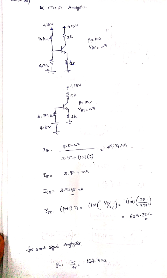
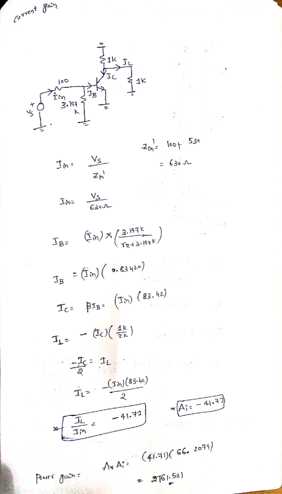
 4. Consider the common-emitter amplifier of Figure 5. Draw the dc circuit and find「CQ. Draw the dc circuit and find ICQ. Find the value of r. Then, calculate values for Voltage gain Av, Open circuit voltage gain Avoc, input impedance Zin, current gain Ai, power gain G, and out- put impedance Zo. Assume operation in the frequency range for which influence of coupling and bypass capacitors can be ignored. +15 V +15 V s in 100Ω CE Figure 5
Font Paragraph Styles 18 Objectives (1) To calculate DC voltages and currents in different sections of...
 Font Paragraph Styles 18 Objectives (1) To calculate DC voltages and currents in different sections of a Common Emitter amplifier. (2) To estimate the voltage gain Av, the input impedance Zin and output impedance Zont of the Common Emitter amplifier. (3) To construct a Common Emitter amplifier circuit on a breadboard. (4) To measure Av, Zin and Zout of the amplifier. Items required 1 Function Generator 1 Variable de power supply 1 Oscilloscope and two scope leads A pair of...
Avec Úvo SRE L V II. (5pt) Consider the above-right common-collector or emitter-follower BJT amplifier circuit....
 Avec Úvo SRE L V II. (5pt) Consider the above-right common-collector or emitter-follower BJT amplifier circuit. Given: ß= 100, RE = 10 k1, Vcc = 20 V, RB = 5 k1, R1 = 10 kl, and Ry = 2 k1. (a) (1pt) Find the Q-point, i.e. Ibo, Ico, and VCEO; (b) (1pt) draw the small-signal equivalent circuit assuming that the capacitors (C, and Cy) are short circuits for the small signal; (c) (1pt) solve for the voltage gain, Av; (d)...
QUESTION 1 Figure Q1 shows a common emitter (CE) and common Base (CB) cascade amplifier circuit....
 QUESTION 1 Figure Q1 shows a common emitter (CE) and common Base (CB) cascade amplifier circuit. Determine the input and output impedance, Z; and Zo, voltage gain, Avi and Av2 and total cascade voltage gain, Ayr and Ays. [25 marks) 2 +8V 1.5 kn 2.2 F 82 k2 3.3 k2 Vo 2.2 uf B = 100 6.8 k12 1 k 2 what B = 100 tuf ZA 5.6 k 2 47012 ZA V. 33 k2 IuF w 10k_2 -2V w...
Can I get help with part g through part r, please? Given the following Common-Emitter Amplifier...
 Can I get help with part g through part r, please?
Given the following Common-Emitter Amplifier with Voltage-Divider Bias: The transistor is a Silicon device with B160 (Beta 160) and transistor r.= 30 kn: 20 V 34.7k LAL = Vou 35.10 31.1k LRE $3900 03 - Find the following quantities in parts a through where means Quiescent DC): a) Thevenin Voltage and Thevenin Resistance Re b) Base Current la Collector Current le d) Emitter Current le e) Transistor Collector-Emitter Quiescent...
Can I get help with part g through part r, please?
Given the following Common-Emitter Amplifier with Voltage-Divider Bias: The transistor is a Silicon device with B160 (Beta 160) and transistor r.= 30 kn: 20 V 34.7k LAL = Vou 35.10 31.1k LRE $3900 03 - Find the following quantities in parts a through where means Quiescent DC): a) Thevenin Voltage and Thevenin Resistance Re b) Base Current la Collector Current le d) Emitter Current le e) Transistor Collector-Emitter Quiescent...
(10 pts) Consider a common-emitter amplifier with emitter resistor shown below. DC voltage source...
 Common-emitter amplifier?
(10 pts) Consider a common-emitter amplifier with emitter resistor shown below. DC voltage sources VBB and Vcc bias the transistor at lc-1mA. Let β-100. Determine the overall voltage gain Gv 2. VCC 10 k2 Vsig VBB
(10 pts) Consider a common-emitter amplifier with emitter resistor shown below. DC voltage sources VBB and Vcc bias the transistor at lc-1mA. Let β-100. Determine the overall voltage gain Gv 2. VCC 10 k2 Vsig VBB
Common-emitter amplifier?
(10 pts) Consider a common-emitter amplifier with emitter resistor shown below. DC voltage sources VBB and Vcc bias the transistor at lc-1mA. Let β-100. Determine the overall voltage gain Gv 2. VCC 10 k2 Vsig VBB
(10 pts) Consider a common-emitter amplifier with emitter resistor shown below. DC voltage sources VBB and Vcc bias the transistor at lc-1mA. Let β-100. Determine the overall voltage gain Gv 2. VCC 10 k2 Vsig VBB
Q1. For the cascade amplifier circuit shown in Fig (1): a) What are the functions of the capacitors C, C2 and C3? And w...
 Q1. For the cascade amplifier circuit shown in Fig (1): a) What are the functions of the capacitors C, C2 and C3? And what are the functions of the capacitors Cs and CE? b) What are the functions of the resistors RD and Rc? c) Draw the DC biasing circuits for each stage. d) Find loa, VGsa, VDs and gm for the JFET stage (you may use either mathematical or graphical methods) e) Calculate l, Ic, le and Ve for...
2.A common-emitter circuit with an emitter bypass capacitor is shown in Figure 2(a) and its small-signal...
 2.A common-emitter circuit with an emitter bypass capacitor is shown in Figure 2(a) and its small-signal equivalent is as in Figure 2(b). Let V' = 10 V, V-=-10 V, RE-4 kQ. Re 2 kQ, CE 50 μF, VED(0) 0.7 V, β 100, VT 0.026 V and VA- Prove that the voltage gain transfer function of the circuit is given by: a) b) Find the values of the time constants τΑ and t, and the corresponding corner frequencies fa and fa....
F LOpoint For the circuit shown in Figure 3 3. 1. Draw the DC equivalent circuit...
 F LOpoint For the circuit shown in Figure 3 3. 1. Draw the DC equivalent circuit by opening caps and shorting inductors 2. Analyze the DC equivalent circuit as we have in previous labs (assume a region, analyze and check assumptions). Check your DC operating point using LT Spice. 3. Calculate the small signal parameters (transconductance, output resistance, input resistance) 4. Draw the AC equivalent circuit by shorting de voltage sources, opening dc current sources, shorting caps and opening inductors....
Shown below is a single stage common emitter amplifier with a unipolar dc power supply using an 2...
 Shown below is a single stage common emitter amplifier with a unipolar dc power supply using an 2N3904 NPN BJT as the active device. It is specified that V+ 40 V, C1 C2CE 100uF, Ro-7.5 k2, REi-5.1kS2, and Ri - 36k52. Design the circuit so that the dc collector current is 2 mA and the magnitude of the small-signal midband voltage gain is 32.3. For the design calculations assume that the base-to- emitter dc voltage drop is 0.65 V, the...
 4. Consider the common-emitter amplifier of Figure 5. Draw the dc circuit and find「CQ. Draw the dc circuit and find ICQ. Find the value of r. Then, calculate values for Voltage gain Av, Open circuit voltage gain Avoc, input impedance Zin, current gain Ai, power gain G, and out- put impedance Zo. Assume operation in the frequency range for which influence of coupling and bypass capacitors can be ignored. +15 V +15 V s in 100Ω CE Figure 5
 Font Paragraph Styles 18 Objectives (1) To calculate DC voltages and currents in different sections of a Common Emitter amplifier. (2) To estimate the voltage gain Av, the input impedance Zin and output impedance Zont of the Common Emitter amplifier. (3) To construct a Common Emitter amplifier circuit on a breadboard. (4) To measure Av, Zin and Zout of the amplifier. Items required 1 Function Generator 1 Variable de power supply 1 Oscilloscope and two scope leads A pair of...
 Avec Úvo SRE L V II. (5pt) Consider the above-right common-collector or emitter-follower BJT amplifier circuit. Given: ß= 100, RE = 10 k1, Vcc = 20 V, RB = 5 k1, R1 = 10 kl, and Ry = 2 k1. (a) (1pt) Find the Q-point, i.e. Ibo, Ico, and VCEO; (b) (1pt) draw the small-signal equivalent circuit assuming that the capacitors (C, and Cy) are short circuits for the small signal; (c) (1pt) solve for the voltage gain, Av; (d)...
 QUESTION 1 Figure Q1 shows a common emitter (CE) and common Base (CB) cascade amplifier circuit. Determine the input and output impedance, Z; and Zo, voltage gain, Avi and Av2 and total cascade voltage gain, Ayr and Ays. [25 marks) 2 +8V 1.5 kn 2.2 F 82 k2 3.3 k2 Vo 2.2 uf B = 100 6.8 k12 1 k 2 what B = 100 tuf ZA 5.6 k 2 47012 ZA V. 33 k2 IuF w 10k_2 -2V w...
 Can I get help with part g through part r, please?
Given the following Common-Emitter Amplifier with Voltage-Divider Bias: The transistor is a Silicon device with B160 (Beta 160) and transistor r.= 30 kn: 20 V 34.7k LAL = Vou 35.10 31.1k LRE $3900 03 - Find the following quantities in parts a through where means Quiescent DC): a) Thevenin Voltage and Thevenin Resistance Re b) Base Current la Collector Current le d) Emitter Current le e) Transistor Collector-Emitter Quiescent...
Can I get help with part g through part r, please?
Given the following Common-Emitter Amplifier with Voltage-Divider Bias: The transistor is a Silicon device with B160 (Beta 160) and transistor r.= 30 kn: 20 V 34.7k LAL = Vou 35.10 31.1k LRE $3900 03 - Find the following quantities in parts a through where means Quiescent DC): a) Thevenin Voltage and Thevenin Resistance Re b) Base Current la Collector Current le d) Emitter Current le e) Transistor Collector-Emitter Quiescent...
 Common-emitter amplifier?
(10 pts) Consider a common-emitter amplifier with emitter resistor shown below. DC voltage sources VBB and Vcc bias the transistor at lc-1mA. Let β-100. Determine the overall voltage gain Gv 2. VCC 10 k2 Vsig VBB
(10 pts) Consider a common-emitter amplifier with emitter resistor shown below. DC voltage sources VBB and Vcc bias the transistor at lc-1mA. Let β-100. Determine the overall voltage gain Gv 2. VCC 10 k2 Vsig VBB
Common-emitter amplifier?
(10 pts) Consider a common-emitter amplifier with emitter resistor shown below. DC voltage sources VBB and Vcc bias the transistor at lc-1mA. Let β-100. Determine the overall voltage gain Gv 2. VCC 10 k2 Vsig VBB
(10 pts) Consider a common-emitter amplifier with emitter resistor shown below. DC voltage sources VBB and Vcc bias the transistor at lc-1mA. Let β-100. Determine the overall voltage gain Gv 2. VCC 10 k2 Vsig VBB
 Q1. For the cascade amplifier circuit shown in Fig (1): a) What are the functions of the capacitors C, C2 and C3? And what are the functions of the capacitors Cs and CE? b) What are the functions of the resistors RD and Rc? c) Draw the DC biasing circuits for each stage. d) Find loa, VGsa, VDs and gm for the JFET stage (you may use either mathematical or graphical methods) e) Calculate l, Ic, le and Ve for...
 2.A common-emitter circuit with an emitter bypass capacitor is shown in Figure 2(a) and its small-signal equivalent is as in Figure 2(b). Let V' = 10 V, V-=-10 V, RE-4 kQ. Re 2 kQ, CE 50 μF, VED(0) 0.7 V, β 100, VT 0.026 V and VA- Prove that the voltage gain transfer function of the circuit is given by: a) b) Find the values of the time constants τΑ and t, and the corresponding corner frequencies fa and fa....
 F LOpoint For the circuit shown in Figure 3 3. 1. Draw the DC equivalent circuit by opening caps and shorting inductors 2. Analyze the DC equivalent circuit as we have in previous labs (assume a region, analyze and check assumptions). Check your DC operating point using LT Spice. 3. Calculate the small signal parameters (transconductance, output resistance, input resistance) 4. Draw the AC equivalent circuit by shorting de voltage sources, opening dc current sources, shorting caps and opening inductors....
 Shown below is a single stage common emitter amplifier with a unipolar dc power supply using an 2N3904 NPN BJT as the active device. It is specified that V+ 40 V, C1 C2CE 100uF, Ro-7.5 k2, REi-5.1kS2, and Ri - 36k52. Design the circuit so that the dc collector current is 2 mA and the magnitude of the small-signal midband voltage gain is 32.3. For the design calculations assume that the base-to- emitter dc voltage drop is 0.65 V, the...
Most questions answered within 3 hours.
-
Write a c/c++ program to read a list of students from a file and
create a...
asked 6 minutes ago -
Identify two different methods for collecting data in
qualitative research. What are the benefits and challenges...
asked 7 minutes ago -
I am suppose to have my array before the main class but I am
getting the...
asked 9 minutes ago -
Your task is to design the page table for the 32bit Pentium
microprocessor. Answer the following...
asked 15 minutes ago -
The Paradise Shoes Company has estimated its weekly TVC function
from data collected over the past...
asked 14 minutes ago -
A researcher wishes to study the cumulative effects of several
combinations of HIV drugs. There are...
asked 14 minutes ago -
Although Epicurus advocates pursuing pleasure for the
good life, discuss a few reasons why he does...
asked 31 minutes ago -
Problem 1: Present entries to record the selected transactions
described below:
(a)
Issued $2,790,000 of 5-year,...
asked 38 minutes ago -
Using technology to support HR activities increases:
a.
the efficiency of the administrative HR functions.
b....
asked 38 minutes ago -
1. List the features used to classify leaf
types.
2. List some characteristics that are shared...
asked 44 minutes ago -
The three elements of Value Proposition, Key Customers, and
Capabilities operate within an environment. Which of...
asked 46 minutes ago -
Katelynn, a physician, earns $200,000 from her medical practice
in the current year. She receives $45,000...
asked 53 minutes ago