How a p-n junction is formed? Explain in full detail indicating reverse bias and forward bias...
How a p-n junction is formed? Explain in full detail indicating reverse bias and forward bias conditions?
Can you explain ?
Homework Answers
Formation of the P-N junction:-
Imagine a thin p-type silicon (p-Si) semiconductor wafer. Now, we add a pentavalent impurity to it. Due to this, a small part of the p-Si wafer is converted into an n-Si. Now, the wafer contains a p-region and an n-region with a metallurgical junction between the two.
(This is one of the simplest way to form p-n junction. Although there re other methods also.)
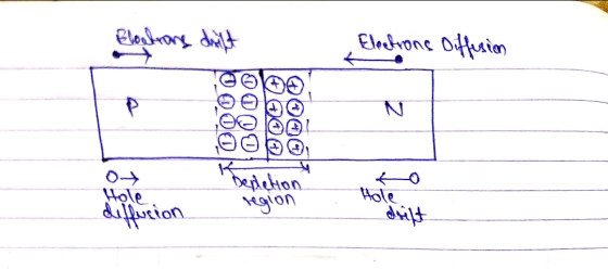
Since the n-type region has a high electron concentration and the p-type a high hole concentration, electrons diffuse from the n-type side to the p-type side. Similarly, holes flow by diffusion from the p-type side to the n-type side.In a p-n junction, when the electrons and holes move to the other side of the junction, they leave behind exposed charges on dopant atom sites, which are fixed in the crystal lattice and are unable to move. On the n-type side, positive ions are exposed. On the p-type side, negative ions are exposed. An electric field forms between the positive ions in the n-type material and negative ions in the p-type material. This region is called the depletion region since the electric field quickly sweeps free carriers out, hence the region is depleted of free carriers.
The current caused by the diffusion of carriers across the junction is called a diffusion current. Minority carriers which reach the edge of the diffusion region are swept across it by the electric field in the depletion region. This current is called the drift current. In equilibrium, the net current from the device is zero. The electron drift current and the electron diffusion current exactly balance out .Similarly, the hole drift current and the hole diffusion current also balance each other out.
( I will include an hand-made diagram at the end which will give you an better idea of diffusion and drift current directions.)
Forward Bias:-
When a diode is connected in a Forward Bias condition, a negative voltage is applied to the N-type material and a positive voltage is applied to the P-type material. If this external voltage becomes greater than the value of the potential barrier, the potential barriers opposition will be overcome and current will start to flow. This is because the negative voltage pushes or repels electrons towards the junction giving them the energy to cross over and combine with the holes being pushed in the opposite direction towards the junction by the positive voltage.
It increases the diffusion current.While the diffusion current increases, the drift current remains essentially unchanged since it depends on the number of carriers generated within a diffusion length of the depletion region or in the depletion region itself. Since the depletion region is only reduced in width by a minor amount, the number of minority carriers swept across the junction is essentially unchanged.
Reverse Bias:-
When a diode is connected in a Reverse Bias condition, a positive voltage is applied to the N-type material and a negative voltage is applied to the P-type material. The positive voltage applied to the N-type material attracts electrons towards the positive electrode and away from the junction, while the holes in the P-type end are also attracted away from the junction towards the negative electrode.
Hence the diffusion current decreases. As in forward bias, the drift current is limited by the number of minority carriers on either side of the p-n junction and is relatively unchanged by the increased electric field. A small increase in the drift current is experienced due to the small increase in the width of the depletion region.
Add Answer to:
How a p-n junction is formed? Explain in full detail indicating
reverse bias and forward bias...
2. An abrupt silicon p-n junction is formed from p-type material with a resistivity of 1.3x10-...
 2. An abrupt silicon p-n junction is formed from p-type material with a resistivity of 1.3x10- 12m and n-type material with resistivity of 4.6x10- Sam at room temperature. The lifetimes of the p- and n-materials are 100 us and 150 us respectively, and the junction area is 1.0 mm?.if Mp 4.8x10² m²/V.s „Mn = 0.135 m²/V.s and n; = 1.5x10¹⁶ carrier /m , calculate the reverse bias leakage current. Then calculate forward bias current if a 0.3 volt is applied.
Biased Sip-n junction A Si p-n junction with area of 0.001 cm* is formed with an acceptor concent...
 Biased Sip-n junction A Si p-n junction with area of 0.001 cm* is formed with an acceptor concentration of Na 1x1015 cm3 on the p-side and a donor concentration of Na- 1x10" cmon the n-side. Calculate at 300 K (a) the diffusion voltage VD (b) the space charge width at equilibrium and with zero bias (c) the current with forward bias of 0.5 eV. Assume that the current is diffusion dominated. The electron and hole mobilities are ln-1500 cm2/(Vs) and...
4. AP-N abrupt junction is formed in Silicon as follows: The P-side has a uniform acceptor...
 4. AP-N abrupt junction is formed in Silicon as follows: The P-side has a uniform acceptor concentration of 2E18/cm^3 and the N-side has a uniform donor concentration of 2E15/cm^3. (a) Find the built-in voltage, V of the P-N junction at 300K. (b) Find the width of the depletion regions in the P and N regions of the transition region for zero reverse bias and for 5V reverse bias. (c) What is the depletion capacitance per unit area with zero reverse...
For an abrupt p-n junction of Area = 10-4 cm2, the measured capacitance under reverse bias...
For an abrupt p-n junction of Area = 10-4 cm2, the measured capacitance under reverse bias of 20 V is 12 pF/cm2. Calculate the donor concentration.
2. For an abrupt p-n junction of area 10^-4 cm^-2, the measured capacitance under reverse bias...
2. For an abrupt p-n junction of area 10^-4 cm^-2, the measured capacitance under reverse bias of 20 V is 12 pF/cm^2. Calculate the donor concentration.
Design an abrupt Si p+-n junction diode that has a reverse breakdown voltage of 130 V and has a forward-bias current of 2.2 mA at V = 0.7 volt. Assume tp = l0^-7 s.
Design an abrupt Sip+-n junction diode that has a reverse breakdown voltage of 130 V andhas a forward-bias current of 2.2 mA at V = 0.7 volt. Assume tp = l0^-7 s.
Explain the origin of leakage current in a reverse-biased p-n junction.
Explain the origin of leakage current in a reverse-biased p-n junction.
3.15 High injection condition The Shockley equation for a pn junction under forward bias, as shown...
 3.15 High injection condition The Shockley equation for a pn junction under forward bias, as shown in Figure 3.16 (a), was derived by assuming low (weak) injection conditions, that is Pn(0) ะ Дрп(0) « nno Or Nd on the n-side. Show that when the injection is no longer weak, that is when p(0) oN, the applied voltage V reaches Vsi (strong injection) given by SI where Vh is the thermal voltage (kgT/e). Calculate V, and Vsi for a Si pn...
Biased Si p-n junction (a) An abrupt Si p-n junction (Schottky model) of square cross section with area of 1x10⁻⁴ cm* has the following properties at 300 K: side Na - 1x1017 cm3 n side Na=1x10¹⁵ -3 c...
 Biased Si p-n junction (a) An abrupt Si p-n junction (Schottky model) of square cross section with area of 1x10⁻⁴ cm* has the following properties at 300 K: side Na - 1x1017 cm3 n side Na=1x10¹⁵ -3 cim =10us 200 cm 2/Vs) In 700 cm2/(Vs) In = 1300 cm 2/(Vs - 450 cm/(Vs) The junction is forward biased by 0.5 V. What is the forward current? (b) What is the current at a reverse bias of-0.5 V?
Biased Si p-n...
Biased Si p-n junction (a) An abrupt Si p-n junction (Schottky model) of square cross section with area of 1x10⁻⁴ cm* has the following properties at 300 K: side Na - 1x1017 cm3 n side Na=1x10¹⁵ -3 cim =10us 200 cm 2/Vs) In 700 cm2/(Vs) In = 1300 cm 2/(Vs - 450 cm/(Vs) The junction is forward biased by 0.5 V. What is the forward current? (b) What is the current at a reverse bias of-0.5 V?
Biased Si p-n...
4- Consider a siliconpn-junction: a) Draw the hand diagram indicating the valence hand, the conduction hand,...
 4- Consider a siliconpn-junction: a) Draw the hand diagram indicating the valence hand, the conduction hand, te rmi energy, and the buil- in potentiul, V ussuming that no voltuge is upplied across the junction. Indicate on this diagram approximately where the depletion region would be. (High level of acuracy is expected in this question). h) The doping is Na = 8x10 I cm? and N, = 2x10 lenN. At 300 K, what is the concentration of holes nn the p-side...
 2. An abrupt silicon p-n junction is formed from p-type material with a resistivity of 1.3x10- 12m and n-type material with resistivity of 4.6x10- Sam at room temperature. The lifetimes of the p- and n-materials are 100 us and 150 us respectively, and the junction area is 1.0 mm?.if Mp 4.8x10² m²/V.s „Mn = 0.135 m²/V.s and n; = 1.5x10¹⁶ carrier /m , calculate the reverse bias leakage current. Then calculate forward bias current if a 0.3 volt is applied.
 Biased Sip-n junction A Si p-n junction with area of 0.001 cm* is formed with an acceptor concentration of Na 1x1015 cm3 on the p-side and a donor concentration of Na- 1x10" cmon the n-side. Calculate at 300 K (a) the diffusion voltage VD (b) the space charge width at equilibrium and with zero bias (c) the current with forward bias of 0.5 eV. Assume that the current is diffusion dominated. The electron and hole mobilities are ln-1500 cm2/(Vs) and...
 4. AP-N abrupt junction is formed in Silicon as follows: The P-side has a uniform acceptor concentration of 2E18/cm^3 and the N-side has a uniform donor concentration of 2E15/cm^3. (a) Find the built-in voltage, V of the P-N junction at 300K. (b) Find the width of the depletion regions in the P and N regions of the transition region for zero reverse bias and for 5V reverse bias. (c) What is the depletion capacitance per unit area with zero reverse...
 3.15 High injection condition The Shockley equation for a pn junction under forward bias, as shown in Figure 3.16 (a), was derived by assuming low (weak) injection conditions, that is Pn(0) ะ Дрп(0) « nno Or Nd on the n-side. Show that when the injection is no longer weak, that is when p(0) oN, the applied voltage V reaches Vsi (strong injection) given by SI where Vh is the thermal voltage (kgT/e). Calculate V, and Vsi for a Si pn...
 Biased Si p-n junction (a) An abrupt Si p-n junction (Schottky model) of square cross section with area of 1x10⁻⁴ cm* has the following properties at 300 K: side Na - 1x1017 cm3 n side Na=1x10¹⁵ -3 cim =10us 200 cm 2/Vs) In 700 cm2/(Vs) In = 1300 cm 2/(Vs - 450 cm/(Vs) The junction is forward biased by 0.5 V. What is the forward current? (b) What is the current at a reverse bias of-0.5 V?
Biased Si p-n...
Biased Si p-n junction (a) An abrupt Si p-n junction (Schottky model) of square cross section with area of 1x10⁻⁴ cm* has the following properties at 300 K: side Na - 1x1017 cm3 n side Na=1x10¹⁵ -3 cim =10us 200 cm 2/Vs) In 700 cm2/(Vs) In = 1300 cm 2/(Vs - 450 cm/(Vs) The junction is forward biased by 0.5 V. What is the forward current? (b) What is the current at a reverse bias of-0.5 V?
Biased Si p-n...
 4- Consider a siliconpn-junction: a) Draw the hand diagram indicating the valence hand, the conduction hand, te rmi energy, and the buil- in potentiul, V ussuming that no voltuge is upplied across the junction. Indicate on this diagram approximately where the depletion region would be. (High level of acuracy is expected in this question). h) The doping is Na = 8x10 I cm? and N, = 2x10 lenN. At 300 K, what is the concentration of holes nn the p-side...
Most questions answered within 3 hours.
-
lease solve all the
questions, don't need to explanations
Q1 - All animal
species have general...
asked 3 hours ago -
Business Phasing
1.Discuss the logical progression for growing a business, which
starts from the initial idea...
asked 3 hours ago -
Modify
When executing on the command line having only
this program name, the program will accept...
asked 5 hours ago -
Kenny Electric Company's noncallable bonds were issued several
years ago and now have 20 years to...
asked 5 hours ago -
find H(e^Jtheta) at theta= 0, pi/10, pi/20, pi/2 for
the following:
a) H(e^Jtheta)= 1+e^Jtheta
b) H(e^Jtheta)=...
asked 5 hours ago -
Home Corporation will open a new store on January 1. Based on
experience from its other...
asked 6 hours ago -
In a neoclassical model, use the IS-LM to analyze the effect of
a permanent money supply...
asked 6 hours ago -
An electron passes through a point 2.67 cm from a long straight
wire as it moves...
asked 7 hours ago -
A grammar is a 4-tuple G, G = (Ν, Σ, Π, Σ, S) where, Ν is...
asked 8 hours ago -
In this part, calculate the present values. Use the Excel PV
function to compute the present...
asked 7 hours ago -
Part 1. Primitive Types, Sorting, Recursion for
Homework.java
a) Implement the static method initializeArray that receives...
asked 9 hours ago -
Using C++, build a sorter that can rank a sequence of numbers in
a descending order....
asked 9 hours ago