
Homework Answers

Add Answer to:
2. An abrupt silicon p-n junction is formed from p-type material with a resistivity of 1.3x10-...
The ratio of hole to electron current for 0.65 V applied bias in a long-base, abrupt p-n junction...
 the ratio of hole to electron current for 0.65 V applied bias in a long-base, abrupt p-n junction de made from silicon having Na-100cm" and Nd-5x10"cm". The carrier lifetimes are 2 μ Sketch the magnitude of the electric field across the junction. [4 pts.]
the ratio of hole to electron current for 0.65 V applied bias in a long-base, abrupt p-n junction de made from silicon having Na-100cm" and Nd-5x10"cm". The carrier lifetimes are 2 μ Sketch the magnitude of...
the ratio of hole to electron current for 0.65 V applied bias in a long-base, abrupt p-n junction de made from silicon having Na-100cm" and Nd-5x10"cm". The carrier lifetimes are 2 μ Sketch the magnitude of the electric field across the junction. [4 pts.]
the ratio of hole to electron current for 0.65 V applied bias in a long-base, abrupt p-n junction de made from silicon having Na-100cm" and Nd-5x10"cm". The carrier lifetimes are 2 μ Sketch the magnitude of...
4. AP-N abrupt junction is formed in Silicon as follows: The P-side has a uniform acceptor...
 4. AP-N abrupt junction is formed in Silicon as follows: The P-side has a uniform acceptor concentration of 2E18/cm^3 and the N-side has a uniform donor concentration of 2E15/cm^3. (a) Find the built-in voltage, V of the P-N junction at 300K. (b) Find the width of the depletion regions in the P and N regions of the transition region for zero reverse bias and for 5V reverse bias. (c) What is the depletion capacitance per unit area with zero reverse...
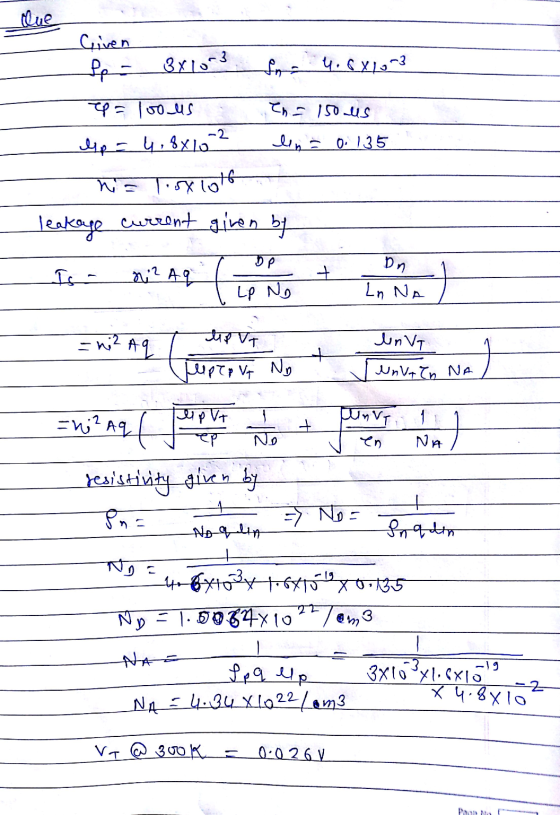
Problem 4: An abrupt silicon p-n junction diode has the following characteristics. side n-side N-4x 1016cm N1016cm3 n 1000 cm2/V sec 350 cm2/V sec Area A 102cm2 Calculate the following quantities...
 Problem 4: An abrupt silicon p-n junction diode has the following characteristics. side n-side N-4x 1016cm N1016cm3 n 1000 cm2/V sec 350 cm2/V sec Area A 102cm2 Calculate the following quantities: (a) Reverse saturation hole current component (b) Reverse saturation electron current component. (c) Minority carrier concentrations at the edge of the depletion layer, p(0) and pr(0), for a forward voltage of 0.6 V (d) Electron and hole current for the bias condition of (c). (e) Make a rough sketch...
Design an ideal abrupt silicon PN-junction at 300 K such that the donor impurity concentration in...
 XXX is 467
Design an ideal abrupt silicon PN-junction at 300 K such that the donor impurity concentration in the n-side N, = 5x1015 cm3 and the acceptor impurity concentration in the p-side N, = XXX × 1015/cm3 Assume that the diode area A-2x10⁻³ cm2 and 100cm work Note that the values obtained in the calculations may not be realistic as the Matric # varies greatly. The assignment is only to test your understanding, and must be handwritten Determine the...
XXX is 467
Design an ideal abrupt silicon PN-junction at 300 K such that the donor impurity concentration in the n-side N, = 5x1015 cm3 and the acceptor impurity concentration in the p-side N, = XXX × 1015/cm3 Assume that the diode area A-2x10⁻³ cm2 and 100cm work Note that the values obtained in the calculations may not be realistic as the Matric # varies greatly. The assignment is only to test your understanding, and must be handwritten Determine the...
A silicon PN junction diode is constructed using N-type silicon in which the Fermi level is...
 A silicon PN junction diode is constructed using N-type silicon in which the Fermi level is 100 meV below the conduction band edge and P-type silicon in which the Fermi level is 120 meV above the valence band edge a) What are the majority and minority carrier concentrations on each side of the junction under thermal equilibrium? b) What is the value of the built-in voltage? c) Determine the width of the depletion region on both sides of the junction...
Assume a p-n step junction in silicon wi concentration of 2x10¹⁶,c? and the n-type material doped...
 Assume a p-n step junction in silicon wi concentration of 2x10¹⁶,c? and the n-type material doped at 3X10-s,cm3 The intrinsic carrier density is 1.25X101°/cm and all dopants are fully ionized Assume that the effective density of states for silicon is 3.3x10 cm3 for the conduction band and 1.75x101 cm for the valence band. Assume that the temperature is 300K and silicon relative permittivity of 11.7 a. Compute the hole concentration on the n-side and electron concentration th the p-type material...
3. A silicon step junction has uniform impurity doping concentrations of N. 5 x 1015 cm-3 and Nd ...
 3. A silicon step junction has uniform impurity doping concentrations of N. 5 x 1015 cm-3 and Nd = 1 x 1015 cm-, and a cross-sectional area of A-|0-4 cm2. Let tao -0.4 s and tpo 0.1 us. Consider the geometry in Figure.Calculate (a) the ideal reverse saturation current due to holes, (b) the ideal reverse saturation current due to electrons, (c) the hole concentration at a, if V V and (d) the electron current at x = x" +...
The depletion width in an abrupt p-n junction is 0.45 μ m at thermal equilibrium. What...
The depletion width in an abrupt p-n junction is 0.45 μ m at thermal equilibrium. What is the new depletion width under a reverse bias voltage of 2 V? The built-in voltage is 0.35V.
2.) Starting with intrinsic silicon with mobilities of n = 1350 cm2 N s and =...
 2.) Starting with intrinsic silicon with mobilities of n = 1350 cm2 N s and = 480 cm2 Nis: a. Find the resistivity p of the silicon. b. If the silicon is now doped with 101/cm-of B (Boron), find the majority and minority carrier concentrations. What is the density of fixed charge in the material (immobile ions)? C. What type of material is this (n type or p type)? d. What is the majority carrier (hole or electron)? e. Find...
Problem 4 (25 points) Consider a silicon pn junction at T-300 K, NA-ND- 1x101° cm3. The minority ...
 Problem 4 (25 points) Consider a silicon pn junction at T-300 K, NA-ND- 1x101° cm3. The minority carrier lifetimes are τ n-0.01 μs and τ p-0.01 us. The junction is forwardbiased with Va 0.6V. The minority carrier diffusion coefficients are Dn-20 cm s, Dp 10 cm Is. n.-1.5x 1010 cm-3 Depletion region n-type p-type a) (10 points) Calculate the excess electron concentration as a function of x in the p side (see the figure above). b) (5 points) Calculate the...
 the ratio of hole to electron current for 0.65 V applied bias in a long-base, abrupt p-n junction de made from silicon having Na-100cm" and Nd-5x10"cm". The carrier lifetimes are 2 μ Sketch the magnitude of the electric field across the junction. [4 pts.]
the ratio of hole to electron current for 0.65 V applied bias in a long-base, abrupt p-n junction de made from silicon having Na-100cm" and Nd-5x10"cm". The carrier lifetimes are 2 μ Sketch the magnitude of...
the ratio of hole to electron current for 0.65 V applied bias in a long-base, abrupt p-n junction de made from silicon having Na-100cm" and Nd-5x10"cm". The carrier lifetimes are 2 μ Sketch the magnitude of the electric field across the junction. [4 pts.]
the ratio of hole to electron current for 0.65 V applied bias in a long-base, abrupt p-n junction de made from silicon having Na-100cm" and Nd-5x10"cm". The carrier lifetimes are 2 μ Sketch the magnitude of...
 4. AP-N abrupt junction is formed in Silicon as follows: The P-side has a uniform acceptor concentration of 2E18/cm^3 and the N-side has a uniform donor concentration of 2E15/cm^3. (a) Find the built-in voltage, V of the P-N junction at 300K. (b) Find the width of the depletion regions in the P and N regions of the transition region for zero reverse bias and for 5V reverse bias. (c) What is the depletion capacitance per unit area with zero reverse...
 Problem 4: An abrupt silicon p-n junction diode has the following characteristics. side n-side N-4x 1016cm N1016cm3 n 1000 cm2/V sec 350 cm2/V sec Area A 102cm2 Calculate the following quantities: (a) Reverse saturation hole current component (b) Reverse saturation electron current component. (c) Minority carrier concentrations at the edge of the depletion layer, p(0) and pr(0), for a forward voltage of 0.6 V (d) Electron and hole current for the bias condition of (c). (e) Make a rough sketch...
 XXX is 467
Design an ideal abrupt silicon PN-junction at 300 K such that the donor impurity concentration in the n-side N, = 5x1015 cm3 and the acceptor impurity concentration in the p-side N, = XXX × 1015/cm3 Assume that the diode area A-2x10⁻³ cm2 and 100cm work Note that the values obtained in the calculations may not be realistic as the Matric # varies greatly. The assignment is only to test your understanding, and must be handwritten Determine the...
XXX is 467
Design an ideal abrupt silicon PN-junction at 300 K such that the donor impurity concentration in the n-side N, = 5x1015 cm3 and the acceptor impurity concentration in the p-side N, = XXX × 1015/cm3 Assume that the diode area A-2x10⁻³ cm2 and 100cm work Note that the values obtained in the calculations may not be realistic as the Matric # varies greatly. The assignment is only to test your understanding, and must be handwritten Determine the...
 A silicon PN junction diode is constructed using N-type silicon in which the Fermi level is 100 meV below the conduction band edge and P-type silicon in which the Fermi level is 120 meV above the valence band edge a) What are the majority and minority carrier concentrations on each side of the junction under thermal equilibrium? b) What is the value of the built-in voltage? c) Determine the width of the depletion region on both sides of the junction...
 Assume a p-n step junction in silicon wi concentration of 2x10¹⁶,c? and the n-type material doped at 3X10-s,cm3 The intrinsic carrier density is 1.25X101°/cm and all dopants are fully ionized Assume that the effective density of states for silicon is 3.3x10 cm3 for the conduction band and 1.75x101 cm for the valence band. Assume that the temperature is 300K and silicon relative permittivity of 11.7 a. Compute the hole concentration on the n-side and electron concentration th the p-type material...
 3. A silicon step junction has uniform impurity doping concentrations of N. 5 x 1015 cm-3 and Nd = 1 x 1015 cm-, and a cross-sectional area of A-|0-4 cm2. Let tao -0.4 s and tpo 0.1 us. Consider the geometry in Figure.Calculate (a) the ideal reverse saturation current due to holes, (b) the ideal reverse saturation current due to electrons, (c) the hole concentration at a, if V V and (d) the electron current at x = x" +...
 2.) Starting with intrinsic silicon with mobilities of n = 1350 cm2 N s and = 480 cm2 Nis: a. Find the resistivity p of the silicon. b. If the silicon is now doped with 101/cm-of B (Boron), find the majority and minority carrier concentrations. What is the density of fixed charge in the material (immobile ions)? C. What type of material is this (n type or p type)? d. What is the majority carrier (hole or electron)? e. Find...
 Problem 4 (25 points) Consider a silicon pn junction at T-300 K, NA-ND- 1x101° cm3. The minority carrier lifetimes are τ n-0.01 μs and τ p-0.01 us. The junction is forwardbiased with Va 0.6V. The minority carrier diffusion coefficients are Dn-20 cm s, Dp 10 cm Is. n.-1.5x 1010 cm-3 Depletion region n-type p-type a) (10 points) Calculate the excess electron concentration as a function of x in the p side (see the figure above). b) (5 points) Calculate the...
Most questions answered within 3 hours.
-
On November 3, the spot price for cotton was $0.81/lb., and the
February futures price was...
asked 4 minutes ago -
Lincoln, Inc., which uses a volume-based cost system, produces
cat condos that sell for $170 each....
asked 3 minutes ago -
Using Python:
A Prime number is an integer greater than 1 that cannot be
formed by...
asked 26 minutes ago -
Read about Cokes strategy in Africa in the article below and
discuss the ethics of selling...
asked 13 minutes ago -
What made of a 40.0% NaOH solution should be diluted to 1.00 L
with water to...
asked 13 minutes ago -
Draw and describe the results of the Meselson-Stahl experiments
showing that DNA replication followed the Semi-conservative...
asked 18 minutes ago -
Deeply Explain the Following Web Development Softwares Along
With the Reasons to Choose them For Development....
asked 15 minutes ago -
essay question: why was Hurricane Katrina so devastating? How
and why did the levees break in...
asked 20 minutes ago -
Why might it be necessary to reduce consumer spending in order
to attain faster economic growth?...
asked 29 minutes ago -
Express your answer with the appropriate units.
1. How many milliliters of oxygen gas at STP...
asked 35 minutes ago -
A
solution is prepared by mixing 0.12L of 0.11 M sodium chloride with
0.26 L of...
asked 37 minutes ago -
Difference between follicle and egg.
Where exactly are LH and FSH located on the ovaries?
What...
asked 37 minutes ago