
Homework Answers

Add Answer to:
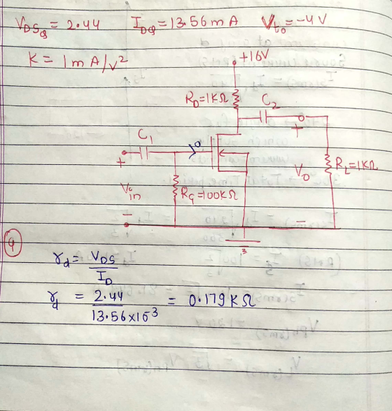
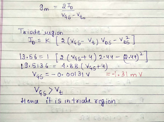
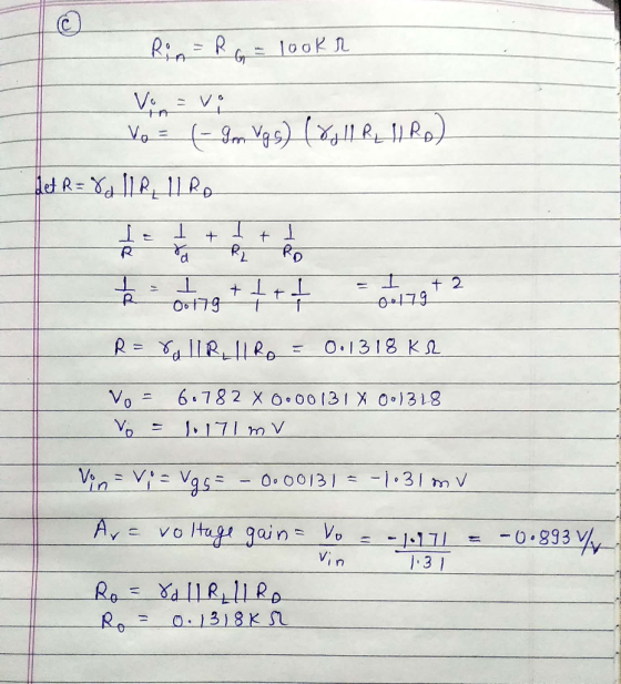
(5) Consider the amplifier shown. Given that V 2.44 V, loo 13.56 mA, and that the...
4) Consider the MOSFET differential amplifier shown below, with Io-2 mA, and RL- 10 kS2, Rss-100 ...
 4) Consider the MOSFET differential amplifier shown below, with Io-2 mA, and RL- 10 kS2, Rss-100 k2, VDD- +8V and Vss--8V. The NMOS transistors in the circuit are nominally identical, with kn 2 mA/V2, VTn 1.0 V and ro 100 k2. The PMoS transistors in the circuit are nominally identical, with kp 2 mA/V2, [VTpl 1.0 V and ro 100 kΩ M3 M4 0 M1 M2 a) First consider the DC bias point. Assuming that the current mirror requires at...
please help with 1&2 Problem i. Common-Gate Amplifier: Assume kp = 2 mA/V, VTp = -1...
 please help with 1&2
Problem i. Common-Gate Amplifier: Assume kp = 2 mA/V, VTp = -1 V.=y=0. Determine the following: (5 pt) 1) Vos and VDS (5 pt) 2) The small-signal parameters, go andro (7.5 pt) 3) Draw small-signal equivalent circuit (7.5 pt) 4) Input Resistance, Rin (7.5 pt) 5) Output Resistance, Rout (15 pt) 6) Small-signal Voltage Gain; A, = Yout +15 V -15 V ima 0 1 ko 50 kn Rout (50 pt) Problem 2. Common-Source Amplifier: Assume...
please help with 1&2
Problem i. Common-Gate Amplifier: Assume kp = 2 mA/V, VTp = -1 V.=y=0. Determine the following: (5 pt) 1) Vos and VDS (5 pt) 2) The small-signal parameters, go andro (7.5 pt) 3) Draw small-signal equivalent circuit (7.5 pt) 4) Input Resistance, Rin (7.5 pt) 5) Output Resistance, Rout (15 pt) 6) Small-signal Voltage Gain; A, = Yout +15 V -15 V ima 0 1 ko 50 kn Rout (50 pt) Problem 2. Common-Source Amplifier: Assume...
Q6. An amplifier circuit using an n-MOSFET is shown in Fig. Q6. The n-MOSFET has the...
 Q6. An amplifier circuit using an n-MOSFET is shown in Fig. Q6. The n-MOSFET has the following parameters: K'-1 mA/V2 and λ-0.02 w. v°' is a small signal AC voltage ource 8V 8V Vout Ra 2.56 mA Fig. Q6 (a) Calculate the DC gate voltage, Va. (b) Assuming that the n-MOSFET is operating in the saturation region and neglecting channel length modulation, calculate the threshold voltage, VrHN, given that the voltage drop across the de current sorce, Inas, has been...
5) Consider the Cascode amplifier shown below. For the NMOS transistors, kn 0.2 mA/V2, Vr,-0.5 V,...
 5) Consider the Cascode amplifier shown below. For the NMOS transistors, kn 0.2 mA/V2, Vr,-0.5 V, (W/L)-(W/L)2-5. VDD-GV and IBIAs= 1.0 mA. a) Assuming λ-0 for all transistors, find the required DC gate- source voltages of M1 and M2 (VGsı and VGs2, respectively) BIAS VD out b) Again assuming 0 M2 for all transistors, what is the minimum DC value of VouT for which the amplifier works in high-gain regime? (W/L)2 in M1 For parts c)-f), Assume -0.01 for all...
QUESTION (1) Transistor Mi in this common base amplifier circuit has the following characteristics: +Vc VTH...
 QUESTION (1) Transistor Mi in this common base amplifier circuit has the following characteristics: +Vc VTH =1 V Rp R, C. K 1 mA/V2 2 0.1 R Given: Vcc 2 mA, 10 V, lbias Ct C2 0, 5 k2, RD 2 k2 RI 10 k, R2 R (12 points) a) Determine the small signal gain, vo/Vin. (4 points) b) Determine the input resistance, Rin. (4 points) c) Determine the output resistance, Ro. Useful formulae: for n-channel MOSFET triode region =...
Design the CS amplifier in Fig. L7.17(a) to achieve a small-signal gain of at least 4,--5 V/V. Us...
 Design the CS amplifier in Fig. L7.17(a) to achieve a small-signal gain of at least 4,--5 V/V. Use supplies of V+--K = 15 V, Rsig-50 Ω, RL-10 kQ, and R1R2 = 10 kQ, and design the circuit to have ID-1 mA and a DC voltage at the gate Vo = 0 V. Use Cc,-CC2-CS-47 μF. What is the expected DC voltage at the source of the NMOS? C1 sig V. Rs sig
Design the CS amplifier in Fig. L7.17(a) to...
Design the CS amplifier in Fig. L7.17(a) to achieve a small-signal gain of at least 4,--5 V/V. Use supplies of V+--K = 15 V, Rsig-50 Ω, RL-10 kQ, and R1R2 = 10 kQ, and design the circuit to have ID-1 mA and a DC voltage at the gate Vo = 0 V. Use Cc,-CC2-CS-47 μF. What is the expected DC voltage at the source of the NMOS? C1 sig V. Rs sig
Design the CS amplifier in Fig. L7.17(a) to...
Q1. For the cascade amplifier circuit shown in Fig (1): a) What are the functions of the capacitors C, C2 and C3? And w...
 Q1. For the cascade amplifier circuit shown in Fig (1): a) What are the functions of the capacitors C, C2 and C3? And what are the functions of the capacitors Cs and CE? b) What are the functions of the resistors RD and Rc? c) Draw the DC biasing circuits for each stage. d) Find loa, VGsa, VDs and gm for the JFET stage (you may use either mathematical or graphical methods) e) Calculate l, Ic, le and Ve for...
uestion 5 marks For the amplifier circuit shown, let Voo -5 V, v-0.7 V, and k-1 mA/V2, the circuit has a voltage gain o...
 uestion 5 marks For the amplifier circuit shown, let Voo -5 V, v-0.7 V, and k-1 mA/V2, the circuit has a voltage gain of (-25 V/V) and an input resistance of (0.5ΜΩ). (a)Calculate Rg and RD (b)Determine Vov,ID (4 Mark) (4 Mark) (c) What is the maximum v,?' d)Sketch v,against voNr Vo ρη
uestion 5 marks For the amplifier circuit shown, let Voo -5 V, v-0.7 V, and k-1 mA/V2, the circuit has a voltage gain of (-25 V/V) and...
uestion 5 marks For the amplifier circuit shown, let Voo -5 V, v-0.7 V, and k-1 mA/V2, the circuit has a voltage gain of (-25 V/V) and an input resistance of (0.5ΜΩ). (a)Calculate Rg and RD (b)Determine Vov,ID (4 Mark) (4 Mark) (c) What is the maximum v,?' d)Sketch v,against voNr Vo ρη
uestion 5 marks For the amplifier circuit shown, let Voo -5 V, v-0.7 V, and k-1 mA/V2, the circuit has a voltage gain of (-25 V/V) and...
In the circuit of given below, Vsig is a small sine wave signal with zero average. The transistor...
 In the circuit of given below, Vsig is a small sine wave signal with zero average. The transistor B is 100. a) Find the value of RE to establish a dc emitter current of about 0.5 mA. b) Find Rc to establish a dc collector voltage of about +5 V c) For RL10 kS2 and the transistor ro 200 k2, draw the small-signal equivalent circuit 5. of the amplifier and determine its overall voltage gain +15 V Re O Vo...
please answer this ASAP Answer the following questions for the below BJT amplifier circuit. Assume capacitors...
 please answer this ASAP
Answer the following questions for the below BJT amplifier circuit. Assume capacitors are short in the signal circuit. Use Vr 25 mV,B = 100, Vpo = 0.7 V, and Ignore the early effect in the bias and signal circuits Find the Bias parameters of the amplifier circuit a) b) Find the small signal parameters of the amplifier. c) Draw the small signal equivalent circuit. Find the open loop voltage gain (Ayo), voltage gain (A,), total circuit...
please answer this ASAP
Answer the following questions for the below BJT amplifier circuit. Assume capacitors are short in the signal circuit. Use Vr 25 mV,B = 100, Vpo = 0.7 V, and Ignore the early effect in the bias and signal circuits Find the Bias parameters of the amplifier circuit a) b) Find the small signal parameters of the amplifier. c) Draw the small signal equivalent circuit. Find the open loop voltage gain (Ayo), voltage gain (A,), total circuit...
 4) Consider the MOSFET differential amplifier shown below, with Io-2 mA, and RL- 10 kS2, Rss-100 k2, VDD- +8V and Vss--8V. The NMOS transistors in the circuit are nominally identical, with kn 2 mA/V2, VTn 1.0 V and ro 100 k2. The PMoS transistors in the circuit are nominally identical, with kp 2 mA/V2, [VTpl 1.0 V and ro 100 kΩ M3 M4 0 M1 M2 a) First consider the DC bias point. Assuming that the current mirror requires at...
 please help with 1&2
Problem i. Common-Gate Amplifier: Assume kp = 2 mA/V, VTp = -1 V.=y=0. Determine the following: (5 pt) 1) Vos and VDS (5 pt) 2) The small-signal parameters, go andro (7.5 pt) 3) Draw small-signal equivalent circuit (7.5 pt) 4) Input Resistance, Rin (7.5 pt) 5) Output Resistance, Rout (15 pt) 6) Small-signal Voltage Gain; A, = Yout +15 V -15 V ima 0 1 ko 50 kn Rout (50 pt) Problem 2. Common-Source Amplifier: Assume...
please help with 1&2
Problem i. Common-Gate Amplifier: Assume kp = 2 mA/V, VTp = -1 V.=y=0. Determine the following: (5 pt) 1) Vos and VDS (5 pt) 2) The small-signal parameters, go andro (7.5 pt) 3) Draw small-signal equivalent circuit (7.5 pt) 4) Input Resistance, Rin (7.5 pt) 5) Output Resistance, Rout (15 pt) 6) Small-signal Voltage Gain; A, = Yout +15 V -15 V ima 0 1 ko 50 kn Rout (50 pt) Problem 2. Common-Source Amplifier: Assume...
 Q6. An amplifier circuit using an n-MOSFET is shown in Fig. Q6. The n-MOSFET has the following parameters: K'-1 mA/V2 and λ-0.02 w. v°' is a small signal AC voltage ource 8V 8V Vout Ra 2.56 mA Fig. Q6 (a) Calculate the DC gate voltage, Va. (b) Assuming that the n-MOSFET is operating in the saturation region and neglecting channel length modulation, calculate the threshold voltage, VrHN, given that the voltage drop across the de current sorce, Inas, has been...
 5) Consider the Cascode amplifier shown below. For the NMOS transistors, kn 0.2 mA/V2, Vr,-0.5 V, (W/L)-(W/L)2-5. VDD-GV and IBIAs= 1.0 mA. a) Assuming λ-0 for all transistors, find the required DC gate- source voltages of M1 and M2 (VGsı and VGs2, respectively) BIAS VD out b) Again assuming 0 M2 for all transistors, what is the minimum DC value of VouT for which the amplifier works in high-gain regime? (W/L)2 in M1 For parts c)-f), Assume -0.01 for all...
 QUESTION (1) Transistor Mi in this common base amplifier circuit has the following characteristics: +Vc VTH =1 V Rp R, C. K 1 mA/V2 2 0.1 R Given: Vcc 2 mA, 10 V, lbias Ct C2 0, 5 k2, RD 2 k2 RI 10 k, R2 R (12 points) a) Determine the small signal gain, vo/Vin. (4 points) b) Determine the input resistance, Rin. (4 points) c) Determine the output resistance, Ro. Useful formulae: for n-channel MOSFET triode region =...
 Design the CS amplifier in Fig. L7.17(a) to achieve a small-signal gain of at least 4,--5 V/V. Use supplies of V+--K = 15 V, Rsig-50 Ω, RL-10 kQ, and R1R2 = 10 kQ, and design the circuit to have ID-1 mA and a DC voltage at the gate Vo = 0 V. Use Cc,-CC2-CS-47 μF. What is the expected DC voltage at the source of the NMOS? C1 sig V. Rs sig
Design the CS amplifier in Fig. L7.17(a) to...
Design the CS amplifier in Fig. L7.17(a) to achieve a small-signal gain of at least 4,--5 V/V. Use supplies of V+--K = 15 V, Rsig-50 Ω, RL-10 kQ, and R1R2 = 10 kQ, and design the circuit to have ID-1 mA and a DC voltage at the gate Vo = 0 V. Use Cc,-CC2-CS-47 μF. What is the expected DC voltage at the source of the NMOS? C1 sig V. Rs sig
Design the CS amplifier in Fig. L7.17(a) to...
 Q1. For the cascade amplifier circuit shown in Fig (1): a) What are the functions of the capacitors C, C2 and C3? And what are the functions of the capacitors Cs and CE? b) What are the functions of the resistors RD and Rc? c) Draw the DC biasing circuits for each stage. d) Find loa, VGsa, VDs and gm for the JFET stage (you may use either mathematical or graphical methods) e) Calculate l, Ic, le and Ve for...
 uestion 5 marks For the amplifier circuit shown, let Voo -5 V, v-0.7 V, and k-1 mA/V2, the circuit has a voltage gain of (-25 V/V) and an input resistance of (0.5ΜΩ). (a)Calculate Rg and RD (b)Determine Vov,ID (4 Mark) (4 Mark) (c) What is the maximum v,?' d)Sketch v,against voNr Vo ρη
uestion 5 marks For the amplifier circuit shown, let Voo -5 V, v-0.7 V, and k-1 mA/V2, the circuit has a voltage gain of (-25 V/V) and...
uestion 5 marks For the amplifier circuit shown, let Voo -5 V, v-0.7 V, and k-1 mA/V2, the circuit has a voltage gain of (-25 V/V) and an input resistance of (0.5ΜΩ). (a)Calculate Rg and RD (b)Determine Vov,ID (4 Mark) (4 Mark) (c) What is the maximum v,?' d)Sketch v,against voNr Vo ρη
uestion 5 marks For the amplifier circuit shown, let Voo -5 V, v-0.7 V, and k-1 mA/V2, the circuit has a voltage gain of (-25 V/V) and...
 In the circuit of given below, Vsig is a small sine wave signal with zero average. The transistor B is 100. a) Find the value of RE to establish a dc emitter current of about 0.5 mA. b) Find Rc to establish a dc collector voltage of about +5 V c) For RL10 kS2 and the transistor ro 200 k2, draw the small-signal equivalent circuit 5. of the amplifier and determine its overall voltage gain +15 V Re O Vo...
 please answer this ASAP
Answer the following questions for the below BJT amplifier circuit. Assume capacitors are short in the signal circuit. Use Vr 25 mV,B = 100, Vpo = 0.7 V, and Ignore the early effect in the bias and signal circuits Find the Bias parameters of the amplifier circuit a) b) Find the small signal parameters of the amplifier. c) Draw the small signal equivalent circuit. Find the open loop voltage gain (Ayo), voltage gain (A,), total circuit...
please answer this ASAP
Answer the following questions for the below BJT amplifier circuit. Assume capacitors are short in the signal circuit. Use Vr 25 mV,B = 100, Vpo = 0.7 V, and Ignore the early effect in the bias and signal circuits Find the Bias parameters of the amplifier circuit a) b) Find the small signal parameters of the amplifier. c) Draw the small signal equivalent circuit. Find the open loop voltage gain (Ayo), voltage gain (A,), total circuit...
Most questions answered within 3 hours.
-
##8. A program contains the following function definition:
##def cube(num):
##return num * num * num...
asked 4 minutes ago -
find the value z of a standard Normal variable that satisfies
each of the given conditions....
asked 27 minutes ago -
"banana".find('z')
Out[22]: -1
why is this -1
python 3.7
asked 8 minutes ago -
Ilegal Consideration Marna Balin was involved in two automobile
accidents in which she suffered severe injures.She...
asked 17 minutes ago -
Walk through the operation of QuickSort when n = 7 and the input
array is A...
asked 12 minutes ago -
Answer with True or False. Argue the answers
7) The circulation of field B on any...
asked 20 minutes ago -
Chase Co. uses the perpetual inventory method. The inventory
records for Chase reflected the following
Jan...
asked 19 minutes ago -
what are is the correct compression for these two ipv6 ips.. i
keep getting them wrong...
asked 23 minutes ago -
How does the amount of silica gel used change separation?
asked 25 minutes ago -
A barium hydroxide solution is prepared by dissolving 1.91 g1.91
g of Ba(OH)2Ba(OH)2 in water to...
asked 43 minutes ago -
barium oxide with water Express your answer as a chemical
equation. Identify all of the phases...
asked 47 minutes ago -
In the laboratory a "coffee cup"
calorimeter, or constant pressure calorimeter, is
frequently used to determine...
asked 45 minutes ago