
Homework Answers


Add Answer to:
3. From the slides and the reference materials, we see that there are two methods for...
why its 4-to-1 mux behavioral? What does the logic circuit represented by the following Verilog module...
 why its 4-to-1 mux behavioral?
What does the logic circuit represented by the following Verilog module do, and what Verilog description style does it use? // My Verilog module #1 module mymodl ( x, d, q) input[1:0] x;input[3:0] d;output q; reg q; wire [1:0] x; wire [3:0] d; always ( x or d) begin case ( x ) 1 : q=d[1]; 2 : g=d[2]; 3 q d[3]; endcase end endmodule
why its 4-to-1 mux behavioral?
What does the logic circuit represented by the following Verilog module do, and what Verilog description style does it use? // My Verilog module #1 module mymodl ( x, d, q) input[1:0] x;input[3:0] d;output q; reg q; wire [1:0] x; wire [3:0] d; always ( x or d) begin case ( x ) 1 : q=d[1]; 2 : g=d[2]; 3 q d[3]; endcase end endmodule
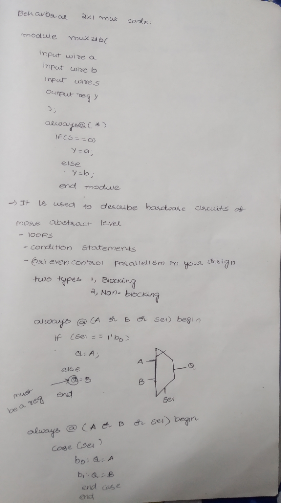
Question 3: Realize the circuit below using Verilog. Include a signal “reset_n” for asynchronously clearing the...
 Question 3: Realize the circuit below using Verilog. Include a signal “reset_n” for asynchronously clearing the flip-flop. What type of circuit is this? Complete the following Verilog code. Write a test bench to test it. clk sel module aff (clk, reset_n, sel, q); input clk ; // Declare the inputs and outputs of the module. input reset_n; input sel; output q; reg q; wire D; ; // model the combinational logic assign D= always @( begin if ( else end...
A specific type of bit-level manipulation consists in setting or clearing one single bit in a...
A specific type of bit-level manipulation consists in setting or clearing one single bit in a multi-bit value, given its index and its new value. This operation can be implemented in hardware by a BitSet circuit with the following interface: Input x is a 4-bit value representing the original value. Output y is a 4-bit value representing the modified value, after the bit-set operation. Input index is a 2-bit value, ranging from 0 to 3, indicating the index of the...
Multiplexer Example Implement the following Boolean function using a 4x1 Mux;
 Multiplexer Example Implement the following Boolean function using a 4x1 Mux; F(x,y,z) = Σ (1,2,6,7) Decoder Example Implement the following functions for a full adder using decoder; S(x,y,z) = Σ (1,2,4,7) C(x,y,z) = Σ (3,5,6,7) Implement the following Boolean function; F(x,y,z) = Σ (0,2,3,7): Using; 1. Two 2x4 decoders and logic gates 2. One 4x1 multiplexer Decoder . Draw the truth table for the function to be implemented. . Pick the terms for output. . Derive appropriate logic to combine terms. . Use two 2x4 decoders to make one3x8 decoder. . Pay attention to fact...
Please solve the problems from 2_5 Digital system Problem 2 Design a combinational circuit with inputs...
 Please solve
the problems from 2_5
Digital
system
Problem 2 Design a combinational circuit with inputs a, b, c, d and outputs w, x, y, z. Assume that the inputs a, b, c d represent a 4-bit signed number (2s complement). The output is also a signed number in 2s complement which is 5 greater than the input if the input is less than 2, and is 2 less than the input if the input is greater than or equal...
Please solve
the problems from 2_5
Digital
system
Problem 2 Design a combinational circuit with inputs a, b, c, d and outputs w, x, y, z. Assume that the inputs a, b, c d represent a 4-bit signed number (2s complement). The output is also a signed number in 2s complement which is 5 greater than the input if the input is less than 2, and is 2 less than the input if the input is greater than or equal...
Can youplease do part b of question 3 (provide a simplified data flow description of the...
 Can youplease do part b of question 3 (provide a simplified data
flow description of the module my foo)
*** I think a mux has to be used..
3. A behavioral model of a combinational circuit is shown below: module myFoo(a,b,C,y); input a,b,c; output y always@(a,b,c) case fa,b 0: y= ~c; 2: y= ~c; A: y=1'b1; endmodule (a) Fill in the missing entries in the code. (b) Provide a simplified data flow description of the module myfoo (3 Points) (4...
Can youplease do part b of question 3 (provide a simplified data
flow description of the module my foo)
*** I think a mux has to be used..
3. A behavioral model of a combinational circuit is shown below: module myFoo(a,b,C,y); input a,b,c; output y always@(a,b,c) case fa,b 0: y= ~c; 2: y= ~c; A: y=1'b1; endmodule (a) Fill in the missing entries in the code. (b) Provide a simplified data flow description of the module myfoo (3 Points) (4...
Please solve the problems from 1_5 Digital system Complete the following homework problems. Show all work...
 Please solve
the problems from 1_5
Digital
system
Complete the following homework problems. Show all work (making sure it is legible) and circle all answers for clarity Problem 1 w3 w4 B w1 a) Determine Boolean functions for intermediate outputs w,w2,w3, and w4 as well as the output signals X and Y. b) Construct a truth table showing the intermediate outputs wl,w2,w3, and w4 as well as the output signals X and Y c) Use K-maps to find simplified expressions...
Please solve
the problems from 1_5
Digital
system
Complete the following homework problems. Show all work (making sure it is legible) and circle all answers for clarity Problem 1 w3 w4 B w1 a) Determine Boolean functions for intermediate outputs w,w2,w3, and w4 as well as the output signals X and Y. b) Construct a truth table showing the intermediate outputs wl,w2,w3, and w4 as well as the output signals X and Y c) Use K-maps to find simplified expressions...
Instantiate four copies of the mux2_1b in mux2_4b file. Connect the 1-bit muxes (4 mux2_1b instances)...
Instantiate four copies of the mux2_1b in mux2_4b file. Connect the 1-bit muxes (4 mux2_1b instances) with ports of mux2_4b to produce 4-bit wide 2:1 multiplexer. This is an example of hierarchical design with reusable modules. The mux2_4b module receives input signals a[3:0], b[3:0], sel, and generates an output signals y[3:0]. I already have a 2_1bit mux verilog coded out but I am not getting correct results intended by what the question is asking. //multiplexer using copies of a mux2:1...
Building and testing basic combinational circuits using Verilog HDL Description: Build and test t...
Building and testing basic combinational circuits using Verilog HDL Description: Build and test the following circuits using gate-level modeling in Verilog HDL. 1. 3-input majority function. 2. Conditional inverter (see the table below: x - control input, y - data input). Do NOT use XOR gates for the implementation. x y Output 0 y 1 y' 3. Two-input multiplexer (see the table below: x,y - data inputs, z - control input). z Output 0 x 1 y 4. 1-bit half...
Please do problem 2 and 3 Complete the following homework problems. Show all work (making answers...
 Please do problem 2 and 3
Complete the following homework problems. Show all work (making answers for clarity sure it is legible) and circle all Problem 1 w3 X A w4 w1 C D Y w2 Determine Boolean functions for intermediate outputs wl,w2,w3, and w4 as well as the output signals X and Y. b) a) Construct a truth table showing the intermediate outputs wl,w2,w3, and w4 as well as the output signals X and Y Use K-maps to find...
Please do problem 2 and 3
Complete the following homework problems. Show all work (making answers for clarity sure it is legible) and circle all Problem 1 w3 X A w4 w1 C D Y w2 Determine Boolean functions for intermediate outputs wl,w2,w3, and w4 as well as the output signals X and Y. b) a) Construct a truth table showing the intermediate outputs wl,w2,w3, and w4 as well as the output signals X and Y Use K-maps to find...
 why its 4-to-1 mux behavioral?
What does the logic circuit represented by the following Verilog module do, and what Verilog description style does it use? // My Verilog module #1 module mymodl ( x, d, q) input[1:0] x;input[3:0] d;output q; reg q; wire [1:0] x; wire [3:0] d; always ( x or d) begin case ( x ) 1 : q=d[1]; 2 : g=d[2]; 3 q d[3]; endcase end endmodule
why its 4-to-1 mux behavioral?
What does the logic circuit represented by the following Verilog module do, and what Verilog description style does it use? // My Verilog module #1 module mymodl ( x, d, q) input[1:0] x;input[3:0] d;output q; reg q; wire [1:0] x; wire [3:0] d; always ( x or d) begin case ( x ) 1 : q=d[1]; 2 : g=d[2]; 3 q d[3]; endcase end endmodule
 Question 3: Realize the circuit below using Verilog. Include a signal “reset_n” for asynchronously clearing the flip-flop. What type of circuit is this? Complete the following Verilog code. Write a test bench to test it. clk sel module aff (clk, reset_n, sel, q); input clk ; // Declare the inputs and outputs of the module. input reset_n; input sel; output q; reg q; wire D; ; // model the combinational logic assign D= always @( begin if ( else end...
 Please solve
the problems from 2_5
Digital
system
Problem 2 Design a combinational circuit with inputs a, b, c, d and outputs w, x, y, z. Assume that the inputs a, b, c d represent a 4-bit signed number (2s complement). The output is also a signed number in 2s complement which is 5 greater than the input if the input is less than 2, and is 2 less than the input if the input is greater than or equal...
Please solve
the problems from 2_5
Digital
system
Problem 2 Design a combinational circuit with inputs a, b, c, d and outputs w, x, y, z. Assume that the inputs a, b, c d represent a 4-bit signed number (2s complement). The output is also a signed number in 2s complement which is 5 greater than the input if the input is less than 2, and is 2 less than the input if the input is greater than or equal...
 Can youplease do part b of question 3 (provide a simplified data
flow description of the module my foo)
*** I think a mux has to be used..
3. A behavioral model of a combinational circuit is shown below: module myFoo(a,b,C,y); input a,b,c; output y always@(a,b,c) case fa,b 0: y= ~c; 2: y= ~c; A: y=1'b1; endmodule (a) Fill in the missing entries in the code. (b) Provide a simplified data flow description of the module myfoo (3 Points) (4...
Can youplease do part b of question 3 (provide a simplified data
flow description of the module my foo)
*** I think a mux has to be used..
3. A behavioral model of a combinational circuit is shown below: module myFoo(a,b,C,y); input a,b,c; output y always@(a,b,c) case fa,b 0: y= ~c; 2: y= ~c; A: y=1'b1; endmodule (a) Fill in the missing entries in the code. (b) Provide a simplified data flow description of the module myfoo (3 Points) (4...
 Please solve
the problems from 1_5
Digital
system
Complete the following homework problems. Show all work (making sure it is legible) and circle all answers for clarity Problem 1 w3 w4 B w1 a) Determine Boolean functions for intermediate outputs w,w2,w3, and w4 as well as the output signals X and Y. b) Construct a truth table showing the intermediate outputs wl,w2,w3, and w4 as well as the output signals X and Y c) Use K-maps to find simplified expressions...
Please solve
the problems from 1_5
Digital
system
Complete the following homework problems. Show all work (making sure it is legible) and circle all answers for clarity Problem 1 w3 w4 B w1 a) Determine Boolean functions for intermediate outputs w,w2,w3, and w4 as well as the output signals X and Y. b) Construct a truth table showing the intermediate outputs wl,w2,w3, and w4 as well as the output signals X and Y c) Use K-maps to find simplified expressions...
 Please do problem 2 and 3
Complete the following homework problems. Show all work (making answers for clarity sure it is legible) and circle all Problem 1 w3 X A w4 w1 C D Y w2 Determine Boolean functions for intermediate outputs wl,w2,w3, and w4 as well as the output signals X and Y. b) a) Construct a truth table showing the intermediate outputs wl,w2,w3, and w4 as well as the output signals X and Y Use K-maps to find...
Please do problem 2 and 3
Complete the following homework problems. Show all work (making answers for clarity sure it is legible) and circle all Problem 1 w3 X A w4 w1 C D Y w2 Determine Boolean functions for intermediate outputs wl,w2,w3, and w4 as well as the output signals X and Y. b) a) Construct a truth table showing the intermediate outputs wl,w2,w3, and w4 as well as the output signals X and Y Use K-maps to find...
Most questions answered within 3 hours.
-
What would you expect the observed boiling point to be at 10
torrs of a liquid...
asked 2 minutes ago -
write a javascript jquery code to display calendar and let it be
sticked on the textbox...
asked 10 minutes ago -
A Call Spread is
A.
The simultaneous purchase of a call and
sale of a put...
asked 10 minutes ago -
In response to concerns about a future recession, the government
decides to give consumers a tax...
asked 11 minutes ago -
Experimental studies of cancer often use strains of animals that
have a naturally high incidence of...
asked 17 minutes ago -
Sociology Question Emile Durkheim
What role does mass media play in the lives of contemporary
citizens?...
asked 22 minutes ago -
Why would you silence gene expression for both wild-type and
mutants? I am on a question...
asked 31 minutes ago -
While all of the elements below are helpful, Booth et al. (2008)
emphasize that it is...
asked 35 minutes ago -
2. Use the three-step method to analyze the effects of the event
on the equilibrium price...
asked 35 minutes ago -
Draw a Venn diagram of three domains of life and explain.
asked 39 minutes ago -
In testing a new drug, researchers found that 5% of all patients
using it will have...
asked 1 hour ago -
List the six general types of information management systems,
and give one logistics application to each...
asked 59 minutes ago