Electronic Circuit Design and Analysis
Please show work to make sure I understand the material! Thanks in advance!
Homework Answers


Add Answer to:
Electronic Circuit Design and Analysis Please show work to make sure I understand the material! T...
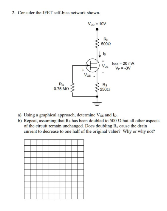
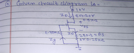
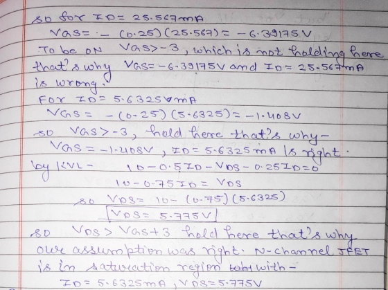
2. Consider the JFET self-bias network shown. VDD 10V 500Ω Vos loss = 20 mA + VGs Rs 2502 0.75 M2...
 2. Consider the JFET self-bias network shown. VDD 10V 500Ω Vos loss = 20 mA + VGs Rs 2502 0.75 M2 a) Using a graphical approach, determine Vos and I b) Repeat, assuming that Rs has been doubled to 500 S2 but all other aspects of the circuit remain unchanged. Does doubling Rs cause the drain current to decrease to one half of the original value? Why or why not?
2. Consider the JFET self-bias network shown. VDD 10V 500Ω...
2. Consider the JFET self-bias network shown. VDD 10V 500Ω Vos loss = 20 mA + VGs Rs 2502 0.75 M2 a) Using a graphical approach, determine Vos and I b) Repeat, assuming that Rs has been doubled to 500 S2 but all other aspects of the circuit remain unchanged. Does doubling Rs cause the drain current to decrease to one half of the original value? Why or why not?
2. Consider the JFET self-bias network shown. VDD 10V 500Ω...
Please help with the LT SPICE for this nmos transistor analysis problem. I figured out the calcul...
 please help with the LT SPICE for this nmos transistor analysis
problem. I figured out the calculations, I just need help verifying
them with LT SPICE. thank you!
Analyze the following MOSFET circuit for dc bias. Solve for ID, VGs and VDs Use RD-5 kQ, Rs-5 kQ, RG,-1 ΜΩ and RG2-1 MS2. Use a power supply with VDD-| 2 V and K.-I mA/V2 and Vin-1 V. RG RD RG2 Rs Verify the analysis of the circuit of Prob. 5 by...
please help with the LT SPICE for this nmos transistor analysis
problem. I figured out the calculations, I just need help verifying
them with LT SPICE. thank you!
Analyze the following MOSFET circuit for dc bias. Solve for ID, VGs and VDs Use RD-5 kQ, Rs-5 kQ, RG,-1 ΜΩ and RG2-1 MS2. Use a power supply with VDD-| 2 V and K.-I mA/V2 and Vin-1 V. RG RD RG2 Rs Verify the analysis of the circuit of Prob. 5 by...
I want help with electronic II . Please answer very clear step by step . Thank...
 I want help with electronic II . Please answer very
clear step by step .
Thank you
2. In the circuit shown, the N-channel JFET amplifier has VGs =-2v, and loss = 5 mA Determine Ip. Vo. Vos: 9m Ay, A and Rin The circuit parameters are as follows: VOD = 20 V, RD = 5 Kn, RG = 200 Kn, Rs = 1 Kn, and Rtoa.-8KI2. out Vin Ro Rs
I want help with electronic II . Please answer very
clear step by step .
Thank you
2. In the circuit shown, the N-channel JFET amplifier has VGs =-2v, and loss = 5 mA Determine Ip. Vo. Vos: 9m Ay, A and Rin The circuit parameters are as follows: VOD = 20 V, RD = 5 Kn, RG = 200 Kn, Rs = 1 Kn, and Rtoa.-8KI2. out Vin Ro Rs
V.+w Operation in the triode reglon Condition v. e Wov 20 Vos uov os os-V (2) p V, so onl+Pala Characteristics Same rel...
 V.+w Operation in the triode reglon Condition v. e Wov 20 Vos uov os os-V (2) p V, so onl+Pala Characteristics Same relationships as for NMOS trasistos tCharacteristics: a CuGs- V,) ®os- } ip.C Replace .and NA with p,,and Nprespectively. V.V V, and yare negative. 2 wov ps For vos 2( -V) e Conditions for operation in the triode region ip lvi Q1. (10 points) For the following configuration of the given figure below, with the following parameters: VDD= +10...
 2. Consider the JFET self-bias network shown. VDD 10V 500Ω Vos loss = 20 mA + VGs Rs 2502 0.75 M2 a) Using a graphical approach, determine Vos and I b) Repeat, assuming that Rs has been doubled to 500 S2 but all other aspects of the circuit remain unchanged. Does doubling Rs cause the drain current to decrease to one half of the original value? Why or why not?
2. Consider the JFET self-bias network shown. VDD 10V 500Ω...
2. Consider the JFET self-bias network shown. VDD 10V 500Ω Vos loss = 20 mA + VGs Rs 2502 0.75 M2 a) Using a graphical approach, determine Vos and I b) Repeat, assuming that Rs has been doubled to 500 S2 but all other aspects of the circuit remain unchanged. Does doubling Rs cause the drain current to decrease to one half of the original value? Why or why not?
2. Consider the JFET self-bias network shown. VDD 10V 500Ω...
 please help with the LT SPICE for this nmos transistor analysis
problem. I figured out the calculations, I just need help verifying
them with LT SPICE. thank you!
Analyze the following MOSFET circuit for dc bias. Solve for ID, VGs and VDs Use RD-5 kQ, Rs-5 kQ, RG,-1 ΜΩ and RG2-1 MS2. Use a power supply with VDD-| 2 V and K.-I mA/V2 and Vin-1 V. RG RD RG2 Rs Verify the analysis of the circuit of Prob. 5 by...
please help with the LT SPICE for this nmos transistor analysis
problem. I figured out the calculations, I just need help verifying
them with LT SPICE. thank you!
Analyze the following MOSFET circuit for dc bias. Solve for ID, VGs and VDs Use RD-5 kQ, Rs-5 kQ, RG,-1 ΜΩ and RG2-1 MS2. Use a power supply with VDD-| 2 V and K.-I mA/V2 and Vin-1 V. RG RD RG2 Rs Verify the analysis of the circuit of Prob. 5 by...
 I want help with electronic II . Please answer very
clear step by step .
Thank you
2. In the circuit shown, the N-channel JFET amplifier has VGs =-2v, and loss = 5 mA Determine Ip. Vo. Vos: 9m Ay, A and Rin The circuit parameters are as follows: VOD = 20 V, RD = 5 Kn, RG = 200 Kn, Rs = 1 Kn, and Rtoa.-8KI2. out Vin Ro Rs
I want help with electronic II . Please answer very
clear step by step .
Thank you
2. In the circuit shown, the N-channel JFET amplifier has VGs =-2v, and loss = 5 mA Determine Ip. Vo. Vos: 9m Ay, A and Rin The circuit parameters are as follows: VOD = 20 V, RD = 5 Kn, RG = 200 Kn, Rs = 1 Kn, and Rtoa.-8KI2. out Vin Ro Rs
 V.+w Operation in the triode reglon Condition v. e Wov 20 Vos uov os os-V (2) p V, so onl+Pala Characteristics Same relationships as for NMOS trasistos tCharacteristics: a CuGs- V,) ®os- } ip.C Replace .and NA with p,,and Nprespectively. V.V V, and yare negative. 2 wov ps For vos 2( -V) e Conditions for operation in the triode region ip lvi Q1. (10 points) For the following configuration of the given figure below, with the following parameters: VDD= +10...
Most questions answered within 3 hours.
-
Calculate the number density of argon gas at a temperature of
24C and a pressure of...
asked 1 hour ago -
Alternative
Classification
How to Estimate
Probabilities from Data? ( For continuous Attributes)
And How to generate...
asked 1 hour ago -
An explosion breaks a 20.0-kg object into three parts. The
object is initially moving at a...
asked 2 hours ago -
Calculate the approximate number of residues of Rubisco, which
is involved in carbon fixation in plants,...
asked 3 hours ago -
Other decisions about scientific claims can have a much broader
impact.ENERGYarrow-10x10.png, environment, health, security - all...
asked 4 hours ago -
I need to write a research paper and work cited about this
topic: The United States...
asked 4 hours ago -
Hello! I was wondering if I could have some help?
If the vapor pressure of carvone...
asked 5 hours ago -
An economist wants to estimate the mean per capita income (in
thousands of dollars) for a...
asked 5 hours ago -
What would be the input/output characteristic of a circuit
obtained by putting two of your 2's-complementers...
asked 5 hours ago -
In Drosophila, the transition from the syncytial blastoderm
stage to the cellular blastoderm stage is a...
asked 5 hours ago -
Project management question:
Name 3 different types of resources (hint: humans are one
type)
asked 6 hours ago -
Consider the following reaction: C 2H 2( g) + 2H 2( g) C 2H 6(
g)...
asked 6 hours ago