
Homework Answers
Add Answer to:
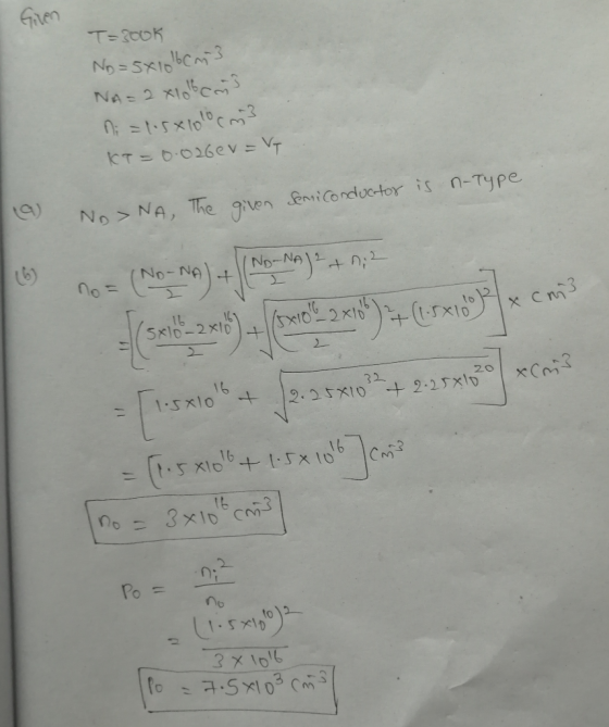
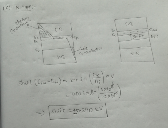
Problem 1 (25 points) Si at T = 300K contains donor impurity atoms at a density of 5x 10'6cm and ...
1. a. Find the main error in each of the band diagrams shown below. For all...
 1. a. Find the main error in each of the band diagrams shown below. For all of the band diagrams Ny 1019/cm3, Ne- 1019/cm3, ni = 3 x 10⁸/cm". E,-1.25 eV, T = 300 K. Ef Ef EFi Main error: Main error: Main error: Main error: Consider a semiconductor sample with the following characteristics: EG 1.25 eV, T 300 K, Nd 5 x 101*/cm3, Na 1014/cm3, N.-1019/cm3, N.-1019/cm3, ni-3 × 10⁸/cm3. Assume complete ionization b. Find the equilibrium electron and...
1. Define the majority carrier concentration in an n-type Si semiconductor in terms of the conduction...
 1. Define the majority carrier concentration in an n-type Si semiconductor in terms of the conduction band edge energy Ec and the Fermi energy Ep 2 marks Find an expression for Ec - Ep, i.e, the difference between the conduction band edge energy and the Fermi energy in terms of the donor concentration Np. 4 marks Determine the concentration of donor impurity atoms that must be added to silicon that Ec Ef = 0.2 eV So 4 marks
Define the majority carrier concentration in an n-type Si semiconductor in terms of the conduction band...
 Define the majority carrier concentration in an n-type Si semiconductor in terms of the conduction band edge energy E, and the Fermi energy E. 1. 2 marks Find an expression for Ee -Ef, i.e, the difference between the conduction band edge energy and the Fermi energy in terms of the donor concentration ND. 4 marks Determine the concentration of donor impurity atoms that must be added to silicon so that Ec- E0.2 eV. 3 marks
Silicon at at T-300 K contains acceptor atoms at a concentration of Na-5x10A15 cmA-3. Donor atoms are added forming an n type compensated(counter doped) semiconductor such that the fermi level is 0.2...
 Silicon at at T-300 K contains acceptor atoms at a concentration of Na-5x10A15 cmA-3. Donor atoms are added forming an n type compensated(counter doped) semiconductor such that the fermi level is 0.215 eV below the conduction band edge 4. a. What concentration of donor atoms were added. b. What were the concentration of holes and electrons before the silicon was counterdoped c. What are the electron and hole concentrations after the silicon was counter doped.
Silicon at at T-300 K...
Silicon at at T-300 K contains acceptor atoms at a concentration of Na-5x10A15 cmA-3. Donor atoms are added forming an n type compensated(counter doped) semiconductor such that the fermi level is 0.215 eV below the conduction band edge 4. a. What concentration of donor atoms were added. b. What were the concentration of holes and electrons before the silicon was counterdoped c. What are the electron and hole concentrations after the silicon was counter doped.
Silicon at at T-300 K...
EENG 245 Physical electronics HW 1 1) The NaCl crystal is cubic, and can be described...
 EENG 245 Physical electronics HW 1 1) The NaCl crystal is cubic, and can be described as follows. Na atoms sit at the corners and faces of a cube, and Cl atoms sit in between two Na atoms. This means that a Clatom is found half-way along each of the cube edges, and there is a Cl in the center of the cube. (We could also have described the lattice by interchanging Na and Cl in the description above.) Another...
For a Si p-n junction with p-type doping of 1 x 10^16/cm3 and n-type doping of...
For a Si p-n junction with p-type doping of 1 x 10^16/cm3 and n-type doping of 1 x 10^19/cm3, calculate the built-in potential Vb at 300K, dark, thermal equilibrium condition. Please show the equations and parameters used in the calculation and the value of Ec-Ef, Ef-Ev, and Vb. Please draw a band structure similar to the one in lecture 5 slide 6 based on your results, please also label Ec, Ev, Vb, and Ef in the drawing.
Electronic ECE
 P and N type semiconductors are formed with an acceptor and donor concentration of 1×1017 cm-3 and 1×1016 cm-3 , respectively,
intrinsic carrier concentration is 1×1010 cm-3 and relative permittivity (єs
) is 12є0 @ 300K.
Given, permittivity of free space (є0
) 8.85 × 10⁻¹² Farad/meter, KT @ 300K 0.0259 eV, q = 1.602 × 10⁻¹⁹ coulombs2. Majority and Minority Electron density (in cm-3
) & Hole density (in cm-3
) under equilibrium B. Draw the following profiles @ 300K 3....
P and N type semiconductors are formed with an acceptor and donor concentration of 1×1017 cm-3 and 1×1016 cm-3 , respectively,
intrinsic carrier concentration is 1×1010 cm-3 and relative permittivity (єs
) is 12є0 @ 300K.
Given, permittivity of free space (є0
) 8.85 × 10⁻¹² Farad/meter, KT @ 300K 0.0259 eV, q = 1.602 × 10⁻¹⁹ coulombs2. Majority and Minority Electron density (in cm-3
) & Hole density (in cm-3
) under equilibrium B. Draw the following profiles @ 300K 3....
14 Q1. Given a NA = 10 /cm" doped Si sample a) b) c) Calculate Ef...
 14 Q1. Given a NA = 10 /cm" doped Si sample a) b) c) Calculate Ef as a function of Temperature T at 500K intervals from 3000K to 5000K. Any conclusion could be drawn from a) part? If the donor has ND-1014/cm3 to replace the NA, what is the Ef at 3000K, 4000K and 5000K The band gap affected by temperature should be included. Q2. At 300K, please find the doping limit of both n-type and p-type Ge to have...
An ideal metal-semiconductor (M-S) junction is formed on the n-type Si semiconductor that is uniformly doped...
 An ideal metal-semiconductor (M-S) junction is formed on the n-type Si semiconductor that is uniformly doped with a donor impurity (phosphorus) concentration of 1016 cm. The metal work function is 4.5 eV, and the Si electron affinity is 4 eV. Assuming that this M-S junction is at 300K, give your best answers to the following questions. (50 points) (a) At thermal equilibrium, draw the energy band diagram including meaningful parameters (energy barriers, energy levels, depletion width, etc.). (b) Calculate the...
 1. a. Find the main error in each of the band diagrams shown below. For all of the band diagrams Ny 1019/cm3, Ne- 1019/cm3, ni = 3 x 10⁸/cm". E,-1.25 eV, T = 300 K. Ef Ef EFi Main error: Main error: Main error: Main error: Consider a semiconductor sample with the following characteristics: EG 1.25 eV, T 300 K, Nd 5 x 101*/cm3, Na 1014/cm3, N.-1019/cm3, N.-1019/cm3, ni-3 × 10⁸/cm3. Assume complete ionization b. Find the equilibrium electron and...
 1. Define the majority carrier concentration in an n-type Si semiconductor in terms of the conduction band edge energy Ec and the Fermi energy Ep 2 marks Find an expression for Ec - Ep, i.e, the difference between the conduction band edge energy and the Fermi energy in terms of the donor concentration Np. 4 marks Determine the concentration of donor impurity atoms that must be added to silicon that Ec Ef = 0.2 eV So 4 marks
 Define the majority carrier concentration in an n-type Si semiconductor in terms of the conduction band edge energy E, and the Fermi energy E. 1. 2 marks Find an expression for Ee -Ef, i.e, the difference between the conduction band edge energy and the Fermi energy in terms of the donor concentration ND. 4 marks Determine the concentration of donor impurity atoms that must be added to silicon so that Ec- E0.2 eV. 3 marks
 Silicon at at T-300 K contains acceptor atoms at a concentration of Na-5x10A15 cmA-3. Donor atoms are added forming an n type compensated(counter doped) semiconductor such that the fermi level is 0.215 eV below the conduction band edge 4. a. What concentration of donor atoms were added. b. What were the concentration of holes and electrons before the silicon was counterdoped c. What are the electron and hole concentrations after the silicon was counter doped.
Silicon at at T-300 K...
Silicon at at T-300 K contains acceptor atoms at a concentration of Na-5x10A15 cmA-3. Donor atoms are added forming an n type compensated(counter doped) semiconductor such that the fermi level is 0.215 eV below the conduction band edge 4. a. What concentration of donor atoms were added. b. What were the concentration of holes and electrons before the silicon was counterdoped c. What are the electron and hole concentrations after the silicon was counter doped.
Silicon at at T-300 K...
 EENG 245 Physical electronics HW 1 1) The NaCl crystal is cubic, and can be described as follows. Na atoms sit at the corners and faces of a cube, and Cl atoms sit in between two Na atoms. This means that a Clatom is found half-way along each of the cube edges, and there is a Cl in the center of the cube. (We could also have described the lattice by interchanging Na and Cl in the description above.) Another...
 14 Q1. Given a NA = 10 /cm" doped Si sample a) b) c) Calculate Ef as a function of Temperature T at 500K intervals from 3000K to 5000K. Any conclusion could be drawn from a) part? If the donor has ND-1014/cm3 to replace the NA, what is the Ef at 3000K, 4000K and 5000K The band gap affected by temperature should be included. Q2. At 300K, please find the doping limit of both n-type and p-type Ge to have...
 An ideal metal-semiconductor (M-S) junction is formed on the n-type Si semiconductor that is uniformly doped with a donor impurity (phosphorus) concentration of 1016 cm. The metal work function is 4.5 eV, and the Si electron affinity is 4 eV. Assuming that this M-S junction is at 300K, give your best answers to the following questions. (50 points) (a) At thermal equilibrium, draw the energy band diagram including meaningful parameters (energy barriers, energy levels, depletion width, etc.). (b) Calculate the...
Most questions answered within 3 hours.
-
a) Find the pressure difference on an airplane wing if air flows
over the upper surface...
asked 1 minute ago -
Write an assessment of the current business analysis of Hilton
Worldwide using Porters 5 Forces analysis.
asked 12 minutes ago -
i need help on this
Chapter 9 Section 3 Question 1:
Rudy puts this poster, with...
asked 20 minutes ago -
True or false Assembly x86
41. _____ The program counter is a pointer to the
instruction....
asked 21 minutes ago -
You have conducted an experiment to try to demonstrate that
growth factor receptor X protein (GFRX)...
asked 36 minutes ago -
The Gross Profit ratio for 2014 is 57.07%
Assume that Campbell's net sales for the first...
asked 36 minutes ago -
Thoroughly discuss the various current and proposed solutions to
anthropogenic influences resulting in Global Climate Change....
asked 40 minutes ago -
BLOG EXERCISE: You are writing a weekly intranet blog for the
CEO of a large Canadian...
asked 43 minutes ago -
calculate ΔGrxn at 36 ∘C. N2O4(g)→2NO2(g)
asked 43 minutes ago -
Present and Future Values of Single Cash Flows for Different
Periods
Find the following values, using...
asked 46 minutes ago -
Which types of mutations in DNA can lead to the translation of a
non-functional protein product?...
asked 45 minutes ago -
Many structures are composed of individual elements that react
in unison when forces are applied. the...
asked 46 minutes ago