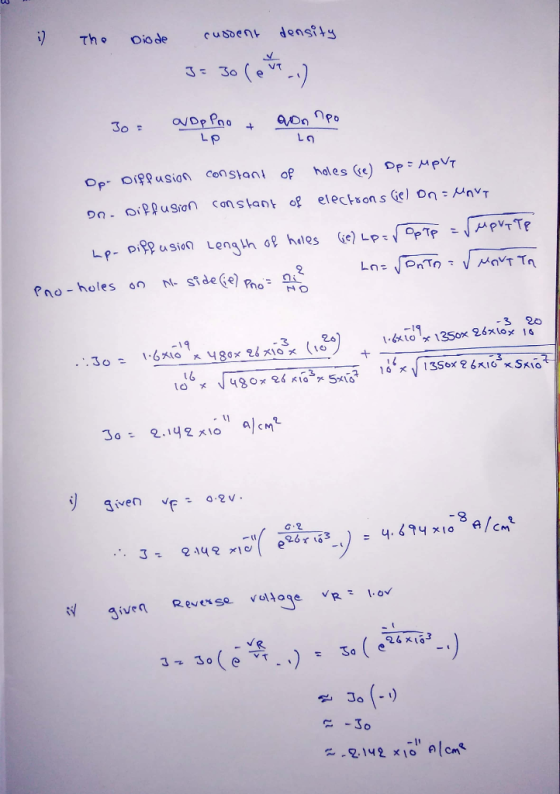
consider a silicon pn junction diode at 300 K with nd= na = 10^16 cm-3, u_n 1350 cm^2/v-s, u_p 480 cm^2/v-s, and t_no = t_po= 5×10^-7 s. consider two bias conditions: i) a reverse bias of 1.0 v ii) a...
consider a silicon pn junction diode at 300 K with nd= na = 10^16 cm-3, u_n 1350 cm^2/v-s, u_p 480 cm^2/v-s, and t_no = t_po= 5×10^-7 s.
consider two bias conditions:
i) a reverse bias of 1.0 v
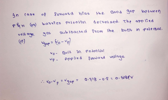
ii) a forward bias of 0.2 v
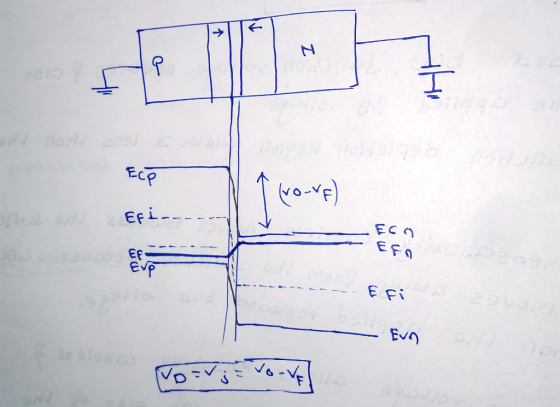
a) for each bus condition, roughly sketch the band gap
diagram
- accurately label the energy gap in eV
- indicate the difference between E_f on the two sides id the
junction and label its value in eV.
b) calculate the "ideal" pn junction current density for this diode under under each bias condition
Homework Answers


Add Answer to:
consider a silicon pn junction diode at 300 K with nd= na = 10^16 cm-3, u_n 1350 cm^2/v-s, u_p 480 cm^2/v-s, and t_no = t_po= 5×10^-7 s. consider two bias conditions: i) a reverse bias of 1.0 v ii) a...
THE REVERSE BIAS VOLTAGE APPLIED TO SILICON PN JUNCTION DIODE IS 4V, DOPING CONCENTRATION Na is...
THE REVERSE BIAS VOLTAGE APPLIED TO SILICON PN JUNCTION DIODE IS 4V, DOPING CONCENTRATION Na is 10^17 cm^-3, Nd = 10^16 cm^-3, ni = 1.3 x 10^9 cm^-3, temperature T = 273 k find the width of depletion region with the applied reverse voltage please check your answer that it is correct please it is a humble request
Design an ideal abrupt silicon PN-junction at 300 K such that the donor impurity concentration in...
 XXX is 467
Design an ideal abrupt silicon PN-junction at 300 K such that the donor impurity concentration in the n-side N, = 5x1015 cm3 and the acceptor impurity concentration in the p-side N, = XXX × 1015/cm3 Assume that the diode area A-2x10⁻³ cm2 and 100cm work Note that the values obtained in the calculations may not be realistic as the Matric # varies greatly. The assignment is only to test your understanding, and must be handwritten Determine the...
XXX is 467
Design an ideal abrupt silicon PN-junction at 300 K such that the donor impurity concentration in the n-side N, = 5x1015 cm3 and the acceptor impurity concentration in the p-side N, = XXX × 1015/cm3 Assume that the diode area A-2x10⁻³ cm2 and 100cm work Note that the values obtained in the calculations may not be realistic as the Matric # varies greatly. The assignment is only to test your understanding, and must be handwritten Determine the...
A silicon pn junction at T = 300 K has the following parameters: Na-5 1016 cm-?,...
 A silicon pn junction at T = 300 K has the following parameters: Na-5 1016 cm-?, N,-1 1016 cm-3, D.-25 cm3/s, D.-10 cm2/s, ?,0-5 x 10⁻⁷ s, and To 1 X 10⁻⁷ s. The cross-sectional area is A 10-3 cm2 and the forward- bias voltage is V,-0.625 V. Calculate the (a) minority electron diffusion cur- rent at the space charge edge, (b) minority hole diffusion current at the space charge edge, and (c) total current in the pn junction diode.
1. Consider a p-n junction diode with doping concentrations: NA6.5x1015 cm3 and ND 107 cm3 in...
 1. Consider a p-n junction diode with doping concentrations: NA6.5x1015 cm3 and ND 107 cm3 in the p- and n-sides, respectively. (a) Calculate the free electron and hole concentrations in both p- and n-sides' neutral regions. (b) Find the barrier height and the built-in voltage. (c) Sketch the energy band diagram of the complete p-n junction. Mark all energy levels including the barrier height and show the energy level values. (d) Calculate the total depletion width under zero bias. (e)...
1. Consider a p*n silicon diode at T-300 K with doping concentrations of N 10 cin...
 1. Consider a p*n silicon diode at T-300 K with doping concentrations of N 10 cin and N-101 cm-3. The minority carier hole diffusion coefficient is D 12 cm2/s and the minority carrier hole lifetime is po 10-7 s. The cross sectional area is A 10- cm2. Calculate the reverse saturation current and the diode current at a forward-bias voltage of 0.50v A germanium p* n diode at T-300 K has the following parameters: Na 108 cm-3 N,--1016 cm", ,...
Consider a silicon pn step junction diode with NA-1x1018 cm3 and No 1x1017cm-3, maintained at T...
 Consider a silicon pn step junction diode with NA-1x1018 cm3 and No 1x1017cm-3, maintained at T 300K. The minority carrier lifetimes in the p-side and n-side are τη-10-8 s and Tp-10-7 s, respectively. a) Calculate the minority carrier densities at the edges of the depletion region when the applied voltage (VA) is 0.6 V. of the junction, for the applied bias voltage of part (a) densities are equal in magnitude, for the applied voltage of part (a). b) Sketch the...
p-side remain unchanged. 3. Consider a long silicon pn junction photodiode at T-300 K with the...
 p-side remain unchanged. 3. Consider a long silicon pn junction photodiode at T-300 K with the following parameters :N, 2x1016 cm-3,Nd-2x1 O18 cm's D,-25 crnVs, D,-10 cm?/sMr-2x10 po-10's. Assume a reverse bias voltage of VR-5 V is applied and assume a uniform generation rate of GL-1021 cm's-1 exists throughout the entire photodiode. Calculate the ratio of the prompt photocurrent density to the total steady state photocurrent density
3. Consider a long silicon pn junction photodiode at T-300 K with the following parameters:N.-2x1016 cm3...
 3. Consider a long silicon pn junction photodiode at T-300 K with the following parameters:N.-2x1016 cm3 Nd 2x1o8 cm3 D.-25 cm2/s, D-10 cmis 2x10s Tpo-10's. Assume a reverse bias voltage of Vx-5 V is applied and assume a uniform generation rate of GL-1021 em's1 exists throughout the entire photodiode.Calculate the ratio of the prompt photocurrent density to the total steady state photocurrem density.
Consider a silicon pn junction at T = 300 K, NA-Np - 4x106cm. The minority carrier...
 Consider a silicon pn junction at T = 300 K, NA-Np - 4x106cm. The minority carrier lifetimes are tn = Tp=1 us. The junction is forward biased with V, -0.6V. The minority carrier diffusion coefficients are D = 20 cm²/s, D = 10 cm²/s. n;= 1.5x100cm, kt/e = 0.026V Depletion region n-type p-type a) (5 points) Do we have low-level injection? b) (10 points) Calculate the electron concentration at x = -(Xp + Ln) where L, is the electron diffusion...
Problem 4 (25 points) Consider a silicon pn junction at T-300 K, NA-ND- 1x101° cm3. The minority ...
 Problem 4 (25 points) Consider a silicon pn junction at T-300 K, NA-ND- 1x101° cm3. The minority carrier lifetimes are τ n-0.01 μs and τ p-0.01 us. The junction is forwardbiased with Va 0.6V. The minority carrier diffusion coefficients are Dn-20 cm s, Dp 10 cm Is. n.-1.5x 1010 cm-3 Depletion region n-type p-type a) (10 points) Calculate the excess electron concentration as a function of x in the p side (see the figure above). b) (5 points) Calculate the...
 XXX is 467
Design an ideal abrupt silicon PN-junction at 300 K such that the donor impurity concentration in the n-side N, = 5x1015 cm3 and the acceptor impurity concentration in the p-side N, = XXX × 1015/cm3 Assume that the diode area A-2x10⁻³ cm2 and 100cm work Note that the values obtained in the calculations may not be realistic as the Matric # varies greatly. The assignment is only to test your understanding, and must be handwritten Determine the...
XXX is 467
Design an ideal abrupt silicon PN-junction at 300 K such that the donor impurity concentration in the n-side N, = 5x1015 cm3 and the acceptor impurity concentration in the p-side N, = XXX × 1015/cm3 Assume that the diode area A-2x10⁻³ cm2 and 100cm work Note that the values obtained in the calculations may not be realistic as the Matric # varies greatly. The assignment is only to test your understanding, and must be handwritten Determine the...
 A silicon pn junction at T = 300 K has the following parameters: Na-5 1016 cm-?, N,-1 1016 cm-3, D.-25 cm3/s, D.-10 cm2/s, ?,0-5 x 10⁻⁷ s, and To 1 X 10⁻⁷ s. The cross-sectional area is A 10-3 cm2 and the forward- bias voltage is V,-0.625 V. Calculate the (a) minority electron diffusion cur- rent at the space charge edge, (b) minority hole diffusion current at the space charge edge, and (c) total current in the pn junction diode.
 1. Consider a p-n junction diode with doping concentrations: NA6.5x1015 cm3 and ND 107 cm3 in the p- and n-sides, respectively. (a) Calculate the free electron and hole concentrations in both p- and n-sides' neutral regions. (b) Find the barrier height and the built-in voltage. (c) Sketch the energy band diagram of the complete p-n junction. Mark all energy levels including the barrier height and show the energy level values. (d) Calculate the total depletion width under zero bias. (e)...
 1. Consider a p*n silicon diode at T-300 K with doping concentrations of N 10 cin and N-101 cm-3. The minority carier hole diffusion coefficient is D 12 cm2/s and the minority carrier hole lifetime is po 10-7 s. The cross sectional area is A 10- cm2. Calculate the reverse saturation current and the diode current at a forward-bias voltage of 0.50v A germanium p* n diode at T-300 K has the following parameters: Na 108 cm-3 N,--1016 cm", ,...
 Consider a silicon pn step junction diode with NA-1x1018 cm3 and No 1x1017cm-3, maintained at T 300K. The minority carrier lifetimes in the p-side and n-side are τη-10-8 s and Tp-10-7 s, respectively. a) Calculate the minority carrier densities at the edges of the depletion region when the applied voltage (VA) is 0.6 V. of the junction, for the applied bias voltage of part (a) densities are equal in magnitude, for the applied voltage of part (a). b) Sketch the...
 p-side remain unchanged. 3. Consider a long silicon pn junction photodiode at T-300 K with the following parameters :N, 2x1016 cm-3,Nd-2x1 O18 cm's D,-25 crnVs, D,-10 cm?/sMr-2x10 po-10's. Assume a reverse bias voltage of VR-5 V is applied and assume a uniform generation rate of GL-1021 cm's-1 exists throughout the entire photodiode. Calculate the ratio of the prompt photocurrent density to the total steady state photocurrent density
 3. Consider a long silicon pn junction photodiode at T-300 K with the following parameters:N.-2x1016 cm3 Nd 2x1o8 cm3 D.-25 cm2/s, D-10 cmis 2x10s Tpo-10's. Assume a reverse bias voltage of Vx-5 V is applied and assume a uniform generation rate of GL-1021 em's1 exists throughout the entire photodiode.Calculate the ratio of the prompt photocurrent density to the total steady state photocurrem density.
 Consider a silicon pn junction at T = 300 K, NA-Np - 4x106cm. The minority carrier lifetimes are tn = Tp=1 us. The junction is forward biased with V, -0.6V. The minority carrier diffusion coefficients are D = 20 cm²/s, D = 10 cm²/s. n;= 1.5x100cm, kt/e = 0.026V Depletion region n-type p-type a) (5 points) Do we have low-level injection? b) (10 points) Calculate the electron concentration at x = -(Xp + Ln) where L, is the electron diffusion...
 Problem 4 (25 points) Consider a silicon pn junction at T-300 K, NA-ND- 1x101° cm3. The minority carrier lifetimes are τ n-0.01 μs and τ p-0.01 us. The junction is forwardbiased with Va 0.6V. The minority carrier diffusion coefficients are Dn-20 cm s, Dp 10 cm Is. n.-1.5x 1010 cm-3 Depletion region n-type p-type a) (10 points) Calculate the excess electron concentration as a function of x in the p side (see the figure above). b) (5 points) Calculate the...
Most questions answered within 3 hours.
-
A 8.15- g bullet from a 9-mm pistol has a velocity of 366.0 m/s.
It strikes...
asked 1 hour ago -
The outstanding bonds of Alpha Extracts have a yield to maturity
of 7.4 percent and a...
asked 1 hour ago -
The Problem: The Case of the Harmonizing Vacations
Your CEO is exploring partnering with a European...
asked 2 hours ago -
A chemical equation is balanced by adding coefficients in front
of some formulas so that the...
asked 2 hours ago -
From the literature (reference your sources): What are the
lattice parameters of calcite and aragonite? Why...
asked 3 hours ago -
Your system is rejecting the question am asking which is
preceded by a case study. It...
asked 3 hours ago -
3. On January 2, 2000, Larry creates a trust with himself as
trustee. Larry as trustee...
asked 3 hours ago -
A member of the volleyball team spikes the ball. During this
process, she changes the velocity...
asked 3 hours ago -
Are adult gamers less likely to use a gaming console (Xbox,
PlayStation, Wii, etc...) than teen...
asked 4 hours ago -
The University of
Texas recently reported that 43% of college students aged 18-24
would spend their...
asked 4 hours ago -
The length of stay at a specific emergency department in
Phoenix, Arizona, in 2009 had a...
asked 3 hours ago -
. Please give the mechanism for this type of problem. Step by
Step
The toxin that...
asked 3 hours ago