Can u answer these questions with explanation!!
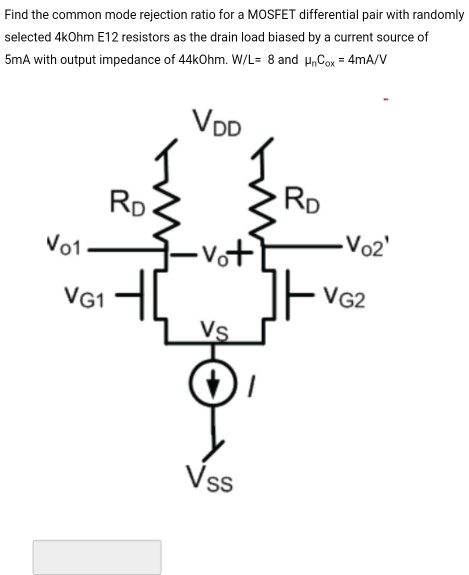
Find the common mode rejection ratio for a MOSFET differential pair with randomly selected 4kOhm E12 resistors as the drain load biased by a current source of 5mA with output impedance of 44kOhm. W/L= 8 and μ.cox-4mA/V VDD RD Vo1 0 VG2 VG1 VSS
Homework Answers

 good luck
Add Answer to:
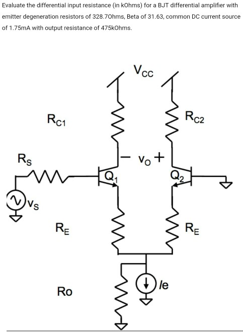
Can u answer these questions with explanation!! Evaluate the differential input resistance (in kOhms) for a BJT differential amplifier with emitter degeneration resistors of 328.70hms, Beta of...
Evaluate the differential input resistance (in kOhms) for a BJT differential amplifier with emitter degeneration resistors of 421.69Ohms, Beta of 66.99, common DC current source of 3.66mA with output...
 Evaluate the differential input resistance (in kOhms) for a BJT differential amplifier with emitter degeneration resistors of 421.69Ohms, Beta of 66.99, common DC current source of 3.66mA with output resistance of 269kOhms. Rct C2 Rs RE le Ro
Evaluate the differential input resistance (in kOhms) for a BJT differential amplifier with emitter degeneration resistors of 421.69Ohms, Beta of 66.99, common DC current source of 3.66mA with output resistance of 269kOhms. Rct C2 Rs RE le Ro
Evaluate the differential input resistance (in kOhms) for a BJT differential amplifier with emitter degeneration resistors of 421.69Ohms, Beta of 66.99, common DC current source of 3.66mA with output resistance of 269kOhms. Rct C2 Rs RE le Ro
Find the common mode rejection ratio in VV for a MOSFET differential pair with randomly selected 9kOhm E12 resistors as the drain load biased by a current source of 2mA with output impedance of 88kOh...
 Find the common mode rejection ratio in VV for a MOSFET differential pair with randomly selected 9kOhm E12 resistors as the drain load biased by a current source of 2mA with output impedance of 88kOhm. W/L 8 and nCox1mA/V RD RD VG2 VG1 Vss
Find the common mode rejection ratio in VV for a MOSFET differential pair with randomly selected 9kOhm E12 resistors as the drain load biased by a current source of 2mA with output impedance of 88kOhm. W/L...
Find the common mode rejection ratio in VV for a MOSFET differential pair with randomly selected 9kOhm E12 resistors as the drain load biased by a current source of 2mA with output impedance of 88kOhm. W/L 8 and nCox1mA/V RD RD VG2 VG1 Vss
Find the common mode rejection ratio in VV for a MOSFET differential pair with randomly selected 9kOhm E12 resistors as the drain load biased by a current source of 2mA with output impedance of 88kOhm. W/L...
4) Consider the MOSFET differential amplifier shown below, with Io-2 mA, and RL- 10 kS2, Rss-100 ...
 4) Consider the MOSFET differential amplifier shown below, with Io-2 mA, and RL- 10 kS2, Rss-100 k2, VDD- +8V and Vss--8V. The NMOS transistors in the circuit are nominally identical, with kn 2 mA/V2, VTn 1.0 V and ro 100 k2. The PMoS transistors in the circuit are nominally identical, with kp 2 mA/V2, [VTpl 1.0 V and ro 100 kΩ M3 M4 0 M1 M2 a) First consider the DC bias point. Assuming that the current mirror requires at...
please answer all spring 2019 Name 19. Gain Margin (dB) is: e1OdByb) 15dBa c) 20 d8;...
 please answer all
spring 2019 Name 19. Gain Margin (dB) is: e1OdByb) 15dBa c) 20 d8; d) 35dB; e) 45d8 20. Phase margin (degree) is close to: a) 0; b) 45pe90) 135) e) 180 21. A MOSFET transistor gm 2m5, Cgs 2pF, Ced 0.5pF, its cut-off frequency, ft, is close to: a) 100 b) 300MHz ) 60OMH)1GHe) SGH 22. The cut-off frequency of a BIT with gm-40m5, r pi-2.5Kohm, r o-20Kohm, c mu 1pF and c pi is close to:...
please answer all
spring 2019 Name 19. Gain Margin (dB) is: e1OdByb) 15dBa c) 20 d8; d) 35dB; e) 45d8 20. Phase margin (degree) is close to: a) 0; b) 45pe90) 135) e) 180 21. A MOSFET transistor gm 2m5, Cgs 2pF, Ced 0.5pF, its cut-off frequency, ft, is close to: a) 100 b) 300MHz ) 60OMH)1GHe) SGH 22. The cut-off frequency of a BIT with gm-40m5, r pi-2.5Kohm, r o-20Kohm, c mu 1pF and c pi is close to:...
Problem 3: Design Problem On Figure P3a, you have a Common Source (CS) n-channel MOSFET amplifier....
 Problem 3: Design Problem On Figure P3a, you have a Common Source (CS) n-channel MOSFET amplifier. Notice the absence of a source resistor Rsig and load resistor R. If we know how the present amplifier (the one on Figure P3a) behaves without Rsig and RL, we can infer its behaviors if Rsig and R were to be added. design the amplifier circuit on Figure P3a, i.e., you have to find appropriate values for RGj You are to RG,, RD, and...
A common source amplifier circuit based on a single n-channel MOSFET is shown in Figure 4b. Assume that the transconductance gm-60 mS (equivalent to mA/ V) and drain source resistance, os,...
 A common source amplifier circuit based on a single n-channel MOSFET is shown in Figure 4b. Assume that the transconductance gm-60 mS (equivalent to mA/ V) and drain source resistance, os, is so large it may be neglected. 0) Calculate the open circuit voltage gain Av Yout/ Vis. i) The amplifier has a load of 10 k2. Determine the current gain Va. = 12 V 150k 4k3 Vout Vin 200k GND = 0 V Figure 4b a) State the name...
 Evaluate the differential input resistance (in kOhms) for a BJT differential amplifier with emitter degeneration resistors of 421.69Ohms, Beta of 66.99, common DC current source of 3.66mA with output resistance of 269kOhms. Rct C2 Rs RE le Ro
Evaluate the differential input resistance (in kOhms) for a BJT differential amplifier with emitter degeneration resistors of 421.69Ohms, Beta of 66.99, common DC current source of 3.66mA with output resistance of 269kOhms. Rct C2 Rs RE le Ro
Evaluate the differential input resistance (in kOhms) for a BJT differential amplifier with emitter degeneration resistors of 421.69Ohms, Beta of 66.99, common DC current source of 3.66mA with output resistance of 269kOhms. Rct C2 Rs RE le Ro
 Find the common mode rejection ratio in VV for a MOSFET differential pair with randomly selected 9kOhm E12 resistors as the drain load biased by a current source of 2mA with output impedance of 88kOhm. W/L 8 and nCox1mA/V RD RD VG2 VG1 Vss
Find the common mode rejection ratio in VV for a MOSFET differential pair with randomly selected 9kOhm E12 resistors as the drain load biased by a current source of 2mA with output impedance of 88kOhm. W/L...
Find the common mode rejection ratio in VV for a MOSFET differential pair with randomly selected 9kOhm E12 resistors as the drain load biased by a current source of 2mA with output impedance of 88kOhm. W/L 8 and nCox1mA/V RD RD VG2 VG1 Vss
Find the common mode rejection ratio in VV for a MOSFET differential pair with randomly selected 9kOhm E12 resistors as the drain load biased by a current source of 2mA with output impedance of 88kOhm. W/L...
 4) Consider the MOSFET differential amplifier shown below, with Io-2 mA, and RL- 10 kS2, Rss-100 k2, VDD- +8V and Vss--8V. The NMOS transistors in the circuit are nominally identical, with kn 2 mA/V2, VTn 1.0 V and ro 100 k2. The PMoS transistors in the circuit are nominally identical, with kp 2 mA/V2, [VTpl 1.0 V and ro 100 kΩ M3 M4 0 M1 M2 a) First consider the DC bias point. Assuming that the current mirror requires at...
 please answer all
spring 2019 Name 19. Gain Margin (dB) is: e1OdByb) 15dBa c) 20 d8; d) 35dB; e) 45d8 20. Phase margin (degree) is close to: a) 0; b) 45pe90) 135) e) 180 21. A MOSFET transistor gm 2m5, Cgs 2pF, Ced 0.5pF, its cut-off frequency, ft, is close to: a) 100 b) 300MHz ) 60OMH)1GHe) SGH 22. The cut-off frequency of a BIT with gm-40m5, r pi-2.5Kohm, r o-20Kohm, c mu 1pF and c pi is close to:...
please answer all
spring 2019 Name 19. Gain Margin (dB) is: e1OdByb) 15dBa c) 20 d8; d) 35dB; e) 45d8 20. Phase margin (degree) is close to: a) 0; b) 45pe90) 135) e) 180 21. A MOSFET transistor gm 2m5, Cgs 2pF, Ced 0.5pF, its cut-off frequency, ft, is close to: a) 100 b) 300MHz ) 60OMH)1GHe) SGH 22. The cut-off frequency of a BIT with gm-40m5, r pi-2.5Kohm, r o-20Kohm, c mu 1pF and c pi is close to:...
 Problem 3: Design Problem On Figure P3a, you have a Common Source (CS) n-channel MOSFET amplifier. Notice the absence of a source resistor Rsig and load resistor R. If we know how the present amplifier (the one on Figure P3a) behaves without Rsig and RL, we can infer its behaviors if Rsig and R were to be added. design the amplifier circuit on Figure P3a, i.e., you have to find appropriate values for RGj You are to RG,, RD, and...
 A common source amplifier circuit based on a single n-channel MOSFET is shown in Figure 4b. Assume that the transconductance gm-60 mS (equivalent to mA/ V) and drain source resistance, os, is so large it may be neglected. 0) Calculate the open circuit voltage gain Av Yout/ Vis. i) The amplifier has a load of 10 k2. Determine the current gain Va. = 12 V 150k 4k3 Vout Vin 200k GND = 0 V Figure 4b a) State the name...
Most questions answered within 3 hours.
-
4. Without doing any calculations, predict whether the observed
∆T would increase, decrease or remain the...
asked 23 minutes ago -
Based on the range, which of the following sets of scores has
the greatest variability? 3,...
asked 1 hour ago -
Ripples in a pond travel at a velocity of 3 m/s with one peak
passing a...
asked 1 hour ago -
A man stands on the roof of a building of height 13.0 mm and
throws a...
asked 1 hour ago -
The extent to which assets are financed by borrowed funds and
other liabilities is indicated by:...
asked 2 hours ago -
Explain in detail
Germany is the fifth largest economy
explain what goods and services Germany specializes...
asked 2 hours ago -
The density of platinum is 21.45 g/mL. If a cube of platinum
with a mass of...
asked 2 hours ago -
Accounts Receivable
Sales
A/R Posting
Extended Sales Invoice
Packing Slip
Compare invoice to packing slip 2...
asked 2 hours ago -
Michaella, age 23, is a full-time law student and is claimed by
her parents as a...
asked 2 hours ago -
Why are polymers not typically casted into products?
asked 3 hours ago -
When rolling a die 129 times, what is the probability of rolling
a 6 no more...
asked 3 hours ago -
4. A call option currently sells for $7.75. It has a strike
price of $85 and...
asked 3 hours ago