
Homework Answers
Add Answer to:
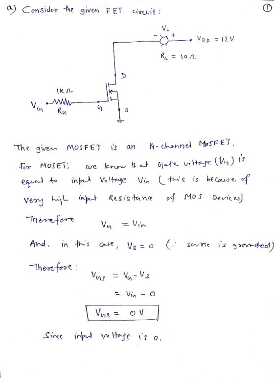
For the figure that is presented, a 10 bulb is connected to the circuit, the power is provided by the field effect transistor. The VDD voltage is 12 V, and RG is 1kQ. When the input voltage (VIN) is...
Observe the circuit presented below. In this circuit appears a motor whose current is 1A and the motor works at a voltage of 12. The voltage of the source (VF) is 12V. Transistor Q1 is a 2N3904. The...
 Observe the circuit presented below. In this circuit appears a motor whose current is 1A and the motor works at a voltage of 12. The voltage of the source (VF) is 12V. Transistor Q1 is a 2N3904. The values of the resistors will be: R1 - 100 kQ, R2 2 kQ, R3 10 kQ. When VIN 0v Find: a) VGS b) ID c) VDS d) VL R2 10 RiN R,
Observe the circuit presented below. In this circuit appears a...
Observe the circuit presented below. In this circuit appears a motor whose current is 1A and the motor works at a voltage of 12. The voltage of the source (VF) is 12V. Transistor Q1 is a 2N3904. The values of the resistors will be: R1 - 100 kQ, R2 2 kQ, R3 10 kQ. When VIN 0v Find: a) VGS b) ID c) VDS d) VL R2 10 RiN R,
Observe the circuit presented below. In this circuit appears a...
4) output and ground is C (not shown). You should add this capacitor in the figure. Assume that the load capacitor connected between the +2.5 V VDD 1.81 Uo 0 2.22 I M When the input voltage changes f...
 4) output and ground is C (not shown). You should add this capacitor in the figure. Assume that the load capacitor connected between the +2.5 V VDD 1.81 Uo 0 2.22 I M When the input voltage changes from VL to VH abruptly at time t 0, (a) In the figure above, draw the path for current flow after the output voltage changes and reaches its new dc value. Draw in the above figure (b) What are the circuit parameters...
V.+w Operation in the triode reglon Condition v. e Wov 20 Vos uov os os-V (2) p V, so onl+Pala Characteristics Same rel...
 V.+w Operation in the triode reglon Condition v. e Wov 20 Vos uov os os-V (2) p V, so onl+Pala Characteristics Same relationships as for NMOS trasistos tCharacteristics: a CuGs- V,) ®os- } ip.C Replace .and NA with p,,and Nprespectively. V.V V, and yare negative. 2 wov ps For vos 2( -V) e Conditions for operation in the triode region ip lvi Q1. (10 points) For the following configuration of the given figure below, with the following parameters: VDD= +10...
Problem 3: Design Problem On Figure P3a, you have a Common Source (CS) n-channel MOSFET amplifier....
 Problem 3: Design Problem On Figure P3a, you have a Common Source (CS) n-channel MOSFET amplifier. Notice the absence of a source resistor Rsig and load resistor R. If we know how the present amplifier (the one on Figure P3a) behaves without Rsig and RL, we can infer its behaviors if Rsig and R were to be added. design the amplifier circuit on Figure P3a, i.e., you have to find appropriate values for RGj You are to RG,, RD, and...
TYU 16.5 Consider the NMOS logic circuit in Figure 16.18. Assume transistor parameters of kn = 10...
 need TYU 16.6
TYU 16.5 Consider the NMOS logic circuit in Figure 16.18. Assume transistor parameters of kn = 100 μ A/ V, and VT = 0.4 V. Assume all driver transistors are identical. Neglect the body effect. (a) If (W/L)L = 0.5, determine (W/L) for the drivers such that VOL(max) = 80μ V. Assume logic 1 input voltages are 2.1 V. 68 Part 3 Digital Electronics VDD = 5 V 0 MDA C DA B DC Figure 16.18 Figure...
need TYU 16.6
TYU 16.5 Consider the NMOS logic circuit in Figure 16.18. Assume transistor parameters of kn = 100 μ A/ V, and VT = 0.4 V. Assume all driver transistors are identical. Neglect the body effect. (a) If (W/L)L = 0.5, determine (W/L) for the drivers such that VOL(max) = 80μ V. Assume logic 1 input voltages are 2.1 V. 68 Part 3 Digital Electronics VDD = 5 V 0 MDA C DA B DC Figure 16.18 Figure...
trical Engineering Il - The ECTPRA2/102/0/2019 EXPERIMENT 4 FIELD EFFECT TRANSISTORS (FETs) RS De Figure 4...
 trical Engineering Il - The ECTPRA2/102/0/2019 EXPERIMENT 4 FIELD EFFECT TRANSISTORS (FETs) RS De Figure 4 Using the Multisim simulation software of whatever version you have (possibly the latest version) connect the circuit in figure 4 above. Use an n-channel JFET model number 2N3821 for the circuit. Do not edit the model parameters of the JFET, use it as it is (5) 42 Connect an ammeter in series with R, to measure the drain current lo, a voltmeter in parallel...
A common source amplifier circuit based on a single n-channel MOSFET is shown in Figure 4b. Assume that the transconductance gm-60 mS (equivalent to mA/ V) and drain source resistance, os,...
 A common source amplifier circuit based on a single n-channel MOSFET is shown in Figure 4b. Assume that the transconductance gm-60 mS (equivalent to mA/ V) and drain source resistance, os, is so large it may be neglected. 0) Calculate the open circuit voltage gain Av Yout/ Vis. i) The amplifier has a load of 10 k2. Determine the current gain Va. = 12 V 150k 4k3 Vout Vin 200k GND = 0 V Figure 4b a) State the name...
 Observe the circuit presented below. In this circuit appears a motor whose current is 1A and the motor works at a voltage of 12. The voltage of the source (VF) is 12V. Transistor Q1 is a 2N3904. The values of the resistors will be: R1 - 100 kQ, R2 2 kQ, R3 10 kQ. When VIN 0v Find: a) VGS b) ID c) VDS d) VL R2 10 RiN R,
Observe the circuit presented below. In this circuit appears a...
Observe the circuit presented below. In this circuit appears a motor whose current is 1A and the motor works at a voltage of 12. The voltage of the source (VF) is 12V. Transistor Q1 is a 2N3904. The values of the resistors will be: R1 - 100 kQ, R2 2 kQ, R3 10 kQ. When VIN 0v Find: a) VGS b) ID c) VDS d) VL R2 10 RiN R,
Observe the circuit presented below. In this circuit appears a...
 4) output and ground is C (not shown). You should add this capacitor in the figure. Assume that the load capacitor connected between the +2.5 V VDD 1.81 Uo 0 2.22 I M When the input voltage changes from VL to VH abruptly at time t 0, (a) In the figure above, draw the path for current flow after the output voltage changes and reaches its new dc value. Draw in the above figure (b) What are the circuit parameters...
 V.+w Operation in the triode reglon Condition v. e Wov 20 Vos uov os os-V (2) p V, so onl+Pala Characteristics Same relationships as for NMOS trasistos tCharacteristics: a CuGs- V,) ®os- } ip.C Replace .and NA with p,,and Nprespectively. V.V V, and yare negative. 2 wov ps For vos 2( -V) e Conditions for operation in the triode region ip lvi Q1. (10 points) For the following configuration of the given figure below, with the following parameters: VDD= +10...
 Problem 3: Design Problem On Figure P3a, you have a Common Source (CS) n-channel MOSFET amplifier. Notice the absence of a source resistor Rsig and load resistor R. If we know how the present amplifier (the one on Figure P3a) behaves without Rsig and RL, we can infer its behaviors if Rsig and R were to be added. design the amplifier circuit on Figure P3a, i.e., you have to find appropriate values for RGj You are to RG,, RD, and...
 need TYU 16.6
TYU 16.5 Consider the NMOS logic circuit in Figure 16.18. Assume transistor parameters of kn = 100 μ A/ V, and VT = 0.4 V. Assume all driver transistors are identical. Neglect the body effect. (a) If (W/L)L = 0.5, determine (W/L) for the drivers such that VOL(max) = 80μ V. Assume logic 1 input voltages are 2.1 V. 68 Part 3 Digital Electronics VDD = 5 V 0 MDA C DA B DC Figure 16.18 Figure...
need TYU 16.6
TYU 16.5 Consider the NMOS logic circuit in Figure 16.18. Assume transistor parameters of kn = 100 μ A/ V, and VT = 0.4 V. Assume all driver transistors are identical. Neglect the body effect. (a) If (W/L)L = 0.5, determine (W/L) for the drivers such that VOL(max) = 80μ V. Assume logic 1 input voltages are 2.1 V. 68 Part 3 Digital Electronics VDD = 5 V 0 MDA C DA B DC Figure 16.18 Figure...
 trical Engineering Il - The ECTPRA2/102/0/2019 EXPERIMENT 4 FIELD EFFECT TRANSISTORS (FETs) RS De Figure 4 Using the Multisim simulation software of whatever version you have (possibly the latest version) connect the circuit in figure 4 above. Use an n-channel JFET model number 2N3821 for the circuit. Do not edit the model parameters of the JFET, use it as it is (5) 42 Connect an ammeter in series with R, to measure the drain current lo, a voltmeter in parallel...
 A common source amplifier circuit based on a single n-channel MOSFET is shown in Figure 4b. Assume that the transconductance gm-60 mS (equivalent to mA/ V) and drain source resistance, os, is so large it may be neglected. 0) Calculate the open circuit voltage gain Av Yout/ Vis. i) The amplifier has a load of 10 k2. Determine the current gain Va. = 12 V 150k 4k3 Vout Vin 200k GND = 0 V Figure 4b a) State the name...
Most questions answered within 3 hours.
-
3) Illustrate the observed pattern of relatedness of organisms
versus adaptations to specific conditions. This means...
asked 8 minutes ago -
In winter a lake has a 0.35 m thick ice layer over 1.10 m of
water....
asked 1 hour ago -
Assuming the following has been encrypted with a Vigenere cipher
below, use the method(s) and assumptions...
asked 1 hour ago -
How would I use switch statements to write a program that will
take an input of...
asked 1 hour ago -
Imagine a reaction in which methane gas combusts at a constant
pressure of 1 atm and...
asked 1 hour ago -
Two parallel wires (each 12 m in length) are separated by a
distance of 0.065 m...
asked 1 hour ago -
Suppose there were three masses at the corner of uniform
equilateral triangle. The masses are m1...
asked 1 hour ago -
Situation: A building that is 618 m above the ground floor. How
many times would a...
asked 1 hour ago -
help me and discuss one successful and one
unsuccessful international company/busines in Indonesia.whyit
succeed and why...
asked 1 hour ago -
I- Choose the best answer
Which of the following statements about the structure and
packaging of...
asked 1 hour ago -
1. A sample of 144 incoming freshman found that 45 of them
scored more than 550...
asked 1 hour ago -
Kc is 2.35 × 10¹⁸ at 25 °C for the formation of iron(III)
oxalate complex ion....
asked 1 hour ago