
Homework Answers

 hope you understand the
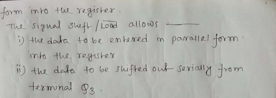
working procedure of a 4 bit parallel in..Serial out shift
register..In above ..
hope you understand the
working procedure of a 4 bit parallel in..Serial out shift
register..In above ..
For any query ask in comment
Add Answer to:
Question 22 (3 marks) What is the function of the circuit shown in Figure 7? D, D, Oo > C FF3 FFI FRO Figure 7 Question 22 (3 marks) What is the function of the circuit shown in Figure 7?...
thx!!!! Question 3 (5.5 marks) a) Find the transfer function of the electrical circuit shown in...
 thx!!!!
Question 3 (5.5 marks) a) Find the transfer function of the electrical circuit shown in Figure 1. What is the value of the steady state gain(s), if any? b) If R1 1, R2 = 2n, C\ = 2- 10-3F, C 1-10-3F, calculate the time constants of the system (if any). c) Find the initial and final values of the unit impulse response of the circuit d) Derive the time-domain expression of the output if the input is the function...
thx!!!!
Question 3 (5.5 marks) a) Find the transfer function of the electrical circuit shown in Figure 1. What is the value of the steady state gain(s), if any? b) If R1 1, R2 = 2n, C\ = 2- 10-3F, C 1-10-3F, calculate the time constants of the system (if any). c) Find the initial and final values of the unit impulse response of the circuit d) Derive the time-domain expression of the output if the input is the function...
Question 1 An electronic circuit is shown in Figure 1. In order to simulate the circuit,...
 Question 1 An electronic circuit is shown in Figure 1. In order to simulate the circuit, a transfer function is needed. a) Is this an open loop or closed loop process? Justify your answer. (3 marks) b) Find the transfer function V.(s) for the electrical network shown in Figure 1. V:(s) (10 marks) c) What is the order of the process? (2 marks) d) Determine the roots of the transfer function and comment on the stability of the process. (5...
Question 3(25 Marks (a) Find the transfer function of the system shown in figure 2 1F 1 Ohm 1F 1 ...
 Question 3(25 Marks (a) Find the transfer function of the system shown in figure 2 1F 1 Ohm 1F 1 Ohm 1 Ohm 1F 1F 1F 1 ohm e Vout Figure 2 (b) Express the transfer function in state space form (c) Use pole placement to determine the gains that will cause the system to have a settling time of 0.1 seconds and an overshoot of 10% (d) Draw an electronic circuit that designed will implement the controller you have...
Question 10 (5 marks) A combinational logic circuit is shown in Figure 3 along with a timing diagram. a) The output waveform (X) shown in the timing diagram is not correct for the circuit shown....
 Question 10 (5 marks) A combinational logic circuit is shown in Figure 3 along with a timing diagram. a) The output waveform (X) shown in the timing diagram is not correct for the circuit shown. Draw the correct waveform. (2 marks) b) The output waveform shown is the result of incorrect implementation of the circuit gates has been replaced by another type of gate. Which gate has been replaced and what is the replacement gate? Explain your answer. (3 marks)...
B. In the circuit in Figure -3, find the value of I, and v [4 Marks]...
 B. In the circuit in Figure -3, find the value of I, and v [4 Marks] In 4k22 3 mv 3 mV i 501, 20k1226 Figure 3 B. In the circuit shown at Figure -6, find the value of Vx due to the 5 A source. [2 marks) 100 a) 40 V b) 50 V c) 15 V d) 22 V = 12v $400 Figure 6
c) For the circuit shown in Figure 3, where u(t) is the unit step function, using...
 c) For the circuit shown in Figure 3, where u(t) is the unit step function, using Laplace transform methods and showing all working, find the response i(t) fort> 0. (9 marks) 4H 7e-u(t) v(1) 352 322 Figure 3
Question 6. (3 marks) Consider the relaxation oscillator circuit shown in Figure 4. Find the time...
 Question 6. (3 marks) Consider the relaxation oscillator circuit shown in Figure 4. Find the time period of the output (which is the output of the op-amp). Assume that the voltage drop across a forward biased diode is negligible. R ? R C = 6 micro-Farad + R= 2 k-Ohm V = 7 volt R1 = 2 k-Ohm R2 = 6 k-Ohm Selected Answer: Correct Answer: 52.7 + 0.5% 52.7 + 0.5% > R2 HHwwKG Figure 4: Circuit for Question...
QUESTION 2 [10 MARKS Assuming the op-amp circuit shown in Figure 2 to be ideal. Find...
 QUESTION 2 [10 MARKS Assuming the op-amp circuit shown in Figure 2 to be ideal. Find the transfer function of the circuit. E,(s) [10 marks] G(s) R3 R1 A B R2 eo(t) e(t) C2 Figure 2 +
When the switch is closed in the circuit shown in the sketch in Figure 22-7
 When the switch is closed in the circuit shown in the sketch in Figure 22-7, the wire between the poles of the horseshoe magnet deflects upward. From this you can conclude that the left end of the magnet is A) a south magnetic pole C) not contributing to the wire's deflection. B) a north magnetic pole. D) a magnetic monopole
The circuit shown in Figure 3 below shows a R-L-C series circuit with components R= 50...
 The circuit shown in Figure 3 below shows a R-L-C series circuit with components R= 50 , L = 1 H, and C= 250 uF. This circuit is connected in series to an AC current source ( il ) where instantaneous current is given by it = 28.29 Sin (100t) A. B + VR- C + VC - D ).4C Current source Figure 3 (a) Draw the circuit diagram for this circuit and mark the impedances (3 marks) (b) What...
 thx!!!!
Question 3 (5.5 marks) a) Find the transfer function of the electrical circuit shown in Figure 1. What is the value of the steady state gain(s), if any? b) If R1 1, R2 = 2n, C\ = 2- 10-3F, C 1-10-3F, calculate the time constants of the system (if any). c) Find the initial and final values of the unit impulse response of the circuit d) Derive the time-domain expression of the output if the input is the function...
thx!!!!
Question 3 (5.5 marks) a) Find the transfer function of the electrical circuit shown in Figure 1. What is the value of the steady state gain(s), if any? b) If R1 1, R2 = 2n, C\ = 2- 10-3F, C 1-10-3F, calculate the time constants of the system (if any). c) Find the initial and final values of the unit impulse response of the circuit d) Derive the time-domain expression of the output if the input is the function...
 Question 1 An electronic circuit is shown in Figure 1. In order to simulate the circuit, a transfer function is needed. a) Is this an open loop or closed loop process? Justify your answer. (3 marks) b) Find the transfer function V.(s) for the electrical network shown in Figure 1. V:(s) (10 marks) c) What is the order of the process? (2 marks) d) Determine the roots of the transfer function and comment on the stability of the process. (5...
 Question 3(25 Marks (a) Find the transfer function of the system shown in figure 2 1F 1 Ohm 1F 1 Ohm 1 Ohm 1F 1F 1F 1 ohm e Vout Figure 2 (b) Express the transfer function in state space form (c) Use pole placement to determine the gains that will cause the system to have a settling time of 0.1 seconds and an overshoot of 10% (d) Draw an electronic circuit that designed will implement the controller you have...
 Question 10 (5 marks) A combinational logic circuit is shown in Figure 3 along with a timing diagram. a) The output waveform (X) shown in the timing diagram is not correct for the circuit shown. Draw the correct waveform. (2 marks) b) The output waveform shown is the result of incorrect implementation of the circuit gates has been replaced by another type of gate. Which gate has been replaced and what is the replacement gate? Explain your answer. (3 marks)...
 B. In the circuit in Figure -3, find the value of I, and v [4 Marks] In 4k22 3 mv 3 mV i 501, 20k1226 Figure 3 B. In the circuit shown at Figure -6, find the value of Vx due to the 5 A source. [2 marks) 100 a) 40 V b) 50 V c) 15 V d) 22 V = 12v $400 Figure 6
 c) For the circuit shown in Figure 3, where u(t) is the unit step function, using Laplace transform methods and showing all working, find the response i(t) fort> 0. (9 marks) 4H 7e-u(t) v(1) 352 322 Figure 3
 Question 6. (3 marks) Consider the relaxation oscillator circuit shown in Figure 4. Find the time period of the output (which is the output of the op-amp). Assume that the voltage drop across a forward biased diode is negligible. R ? R C = 6 micro-Farad + R= 2 k-Ohm V = 7 volt R1 = 2 k-Ohm R2 = 6 k-Ohm Selected Answer: Correct Answer: 52.7 + 0.5% 52.7 + 0.5% > R2 HHwwKG Figure 4: Circuit for Question...
 QUESTION 2 [10 MARKS Assuming the op-amp circuit shown in Figure 2 to be ideal. Find the transfer function of the circuit. E,(s) [10 marks] G(s) R3 R1 A B R2 eo(t) e(t) C2 Figure 2 +
 The circuit shown in Figure 3 below shows a R-L-C series circuit with components R= 50 , L = 1 H, and C= 250 uF. This circuit is connected in series to an AC current source ( il ) where instantaneous current is given by it = 28.29 Sin (100t) A. B + VR- C + VC - D ).4C Current source Figure 3 (a) Draw the circuit diagram for this circuit and mark the impedances (3 marks) (b) What...
Most questions answered within 3 hours.
-
Using MARS simulator, write MIPS programs according to
the following scenarios: Receive a positive integer number...
asked 13 minutes ago -
An object in front of a concave mirror has a real image that is
11.5 cm...
asked 26 minutes ago -
Consider the reaction, C3 H8 + O2 --> CO2 + H2O. How many
moles of O2...
asked 2 hours ago -
You and your opponent both roll a fair die. If you both roll the
same number,...
asked 2 hours ago -
In a study of the accuracy of fast food drive-through orders,
Restaurant A had 257 accurate...
asked 2 hours ago -
Identify and describe in detail the four categories of
institutions that could be included in a...
asked 2 hours ago -
In python
class Customer:
def __init__(self, customer_id, last_name, first_name, phone_number, address):
self._customer_id = int(customer_id)
self._last_name =...
asked 2 hours ago -
What is an example of a limitation in implementing a new
ERP system and how it...
asked 2 hours ago -
In a section of 9.7cm of an artery with a radius of 2.6mm there
is a...
asked 2 hours ago -
the two carboxylic acid groups of aspartic acid have different
acidities with pKa values of 2.1...
asked 2 hours ago -
Would CuCO3 aqueous salt combined with calcium chloride
form a solid precipitate? If so, what would...
asked 2 hours ago -
How do ECM Solutions assist in embedding a culture of continuous
improvement in an organization? (Project...
asked 3 hours ago