
Homework Answers
Add Answer to:
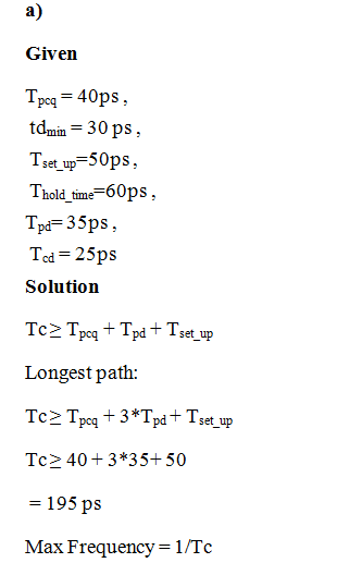
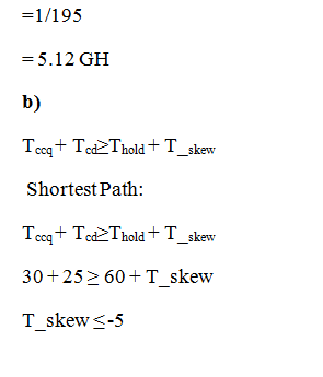
(20 pts.) For the following circuit, the timing characteristics of the components are summarized below. .Flip-flop:...
Name: (4) (10 pts) Design a Moore FSM that has one input A and one output Y, and the output Y should be 1 if A has...
 Name: (4) (10 pts) Design a Moore FSM that has one input A and one output Y, and the output Y should be 1 if A has been 101 during the most recent three consecutive clock cycles or A has been 1 during the two most recent consecutive clock cycles. You only need to write down your state transition diagram. (5) (6 pts) Consider the following sequential circuit. Each two-input OR gate has a propagation delay of 130ps and a...
3. (16 pts.) A sequential circuit design is shown in the following diagram CLK CLK Frt Trl Frl FF1 D-FF clk-to-q propagation delay tpcq 15 ps D-FF clk-to-q contamination delay tccq-10 ps D-FF dat...
 3. (16 pts.) A sequential circuit design is shown in the following diagram CLK CLK Frt Trl Frl FF1 D-FF clk-to-q propagation delay tpcq 15 ps D-FF clk-to-q contamination delay tccq-10 ps D-FF data setup time ts-15 ps D-FF data hold time th = 10 ps Gate 2-input NAND 2-input NOR 2-input XOIR NOT Tpd(ps) Tea(ps) 15 25 35 10 10 15 25 (8 pts.) Calculate the maximum clock frequency for reliable operation assuming there is no clock skew (8...
Design an electronic lock system. This system has 2 inputs: A and B. This system will...
 Design an electronic lock system. This system has 2 inputs: A and B. This system will be unlocked when the sequence BBA is pressed. State diagram of this electronic lock system is shown below. - Draw a circuit diagram and find the maximum clock frequency of your circuit. Check if this circuit violates any hold time violation Note: 1) This circuit is a Moore machine 2) Please assign each state as follows, XO = 00, x1 = 01, X2 =...
(b) Using a timing diagram showing the clk, Q1 and D2 signals, explain the following timing const...
 (b) Using a timing diagram showing the clk, Q1 and D2 signals, explain the following timing constraints for the circuit shown in Figure 2.1 cqtcd 2 old where tod is the contamination delay of the combinational logic 7 marks reg2 reg1 Combinational D2 logic clk. clk Figure 2.1 (c) In the circuit shown in Figure 2.2, the flip-flops have a clock-to-Q contamination delay of 30 ps and a propagation delay of 80 ps. They have a setup time of 50...
TIMING Consider the following ciru. The clock connections to the flip-flops are not shown (both flip-flops...
 TIMING Consider the following ciru. The clock connections to the flip-flops are not shown (both flip-flops are clocked by the same clock). Y1 D a Assume the following Delay of each AND gate: 1 ns Delay of each inverter 04 ns Set up time of each flip-flop: 0.1 ns Hold time of each flip-flop: 0 ns Clk-to-Q delay of each fip-flop: 0.3 ns a) What is the maximum frequency of the clock in this cicuit (in MHz)? b) Suppose the...
Study the following circuit and corresponding waveforms: a) D Q Clock CLK Q Undefined 01 02...
 Study the following circuit and corresponding waveforms: a) D Q Clock CLK Q Undefined 01 02 Undefined Q Undefined Undefined Undefined Identify the waveforms that correspond to Qa, Qb and Qc. Provide the name of the components that produce Qa, Qb and Qc. (Note: one answer is none of the above.) (6 marks) b) Study the following circuit: D D D CLK CLK CLK CLK Explain why this will not implement a shift register. Your answer should include a waveform...
Given the register/combinational logic circuitry below, determine if the setup time constraint and hold time constraint...
 Given the register/combinational logic circuitry below, determine if the setup time constraint and hold time constraint are met. If not, what can be done? What is the maximum clock frequency allowed? Given: Timing characteristics of the registers (Flip Flops): CLK1 CLK2 tsu 55 ps(setup time) th 70ps (hold time) teq -30 ps (contamination delay) toce 45 ps (propagation delay) Timing characteristics of each gate: tpd 35 ps (propagation delay) ted 20 ps (contamination delay) The skew between the two clocks...
Consider the circuit shown below. The blocks A, B and C represent combination logic blocks with t...
 Consider the circuit shown below. The blocks A, B and C represent combination logic blocks with the following propagation delays: tAmin-100ps, tAmax400ps, ts.min -30ps, tB,max700ps t,min 60ps, tcmax 200ps, where tmin is the minimum delay while tmax is the maximum Blocks L1 and L2 are rising edge triggered registers clocked by φ. These two registers are identical and have a setup- a) (5 pts) Determine whether this circuit has a hold time violation. Explain why. b) (5 pts) Find the...
(e) Suppose that for the circuit of Figure 11-21, new semiconductor technol- ogy has allowed us...
 (e) Suppose that for the circuit of Figure 11-21, new semiconductor technol- ogy has allowed us to improve the delays and setup times. The propagation delay of the new inverter is 1.5 ns, and the propagation delay and setup times of the new flip-flop are 3.5 ns and 2 ns, respectively. What is the short- est clock period for the circuit of Figure 11-21(a) which will not violate the timing constraints? Setup time 3 si CLK FIGURE 11-21 Determination of...
3) Recall that a flip-flop is built from 2 latches cascaded in the master-slave configuration as...
 3) Recall that a flip-flop is built from 2 latches cascaded in the master-slave configuration as shown in Figure S. Assume that each latch has a D-to-Q propagation delay of 5ns and a D to-Q contamination delay of 2ns. The inverter has a propagation delay of 5ns and a contamination delay of ens. If you were the designer of this flip-flop, what would you report as the setup time and hold time of the flip-flop? D latch (master) D latch...
 Name: (4) (10 pts) Design a Moore FSM that has one input A and one output Y, and the output Y should be 1 if A has been 101 during the most recent three consecutive clock cycles or A has been 1 during the two most recent consecutive clock cycles. You only need to write down your state transition diagram. (5) (6 pts) Consider the following sequential circuit. Each two-input OR gate has a propagation delay of 130ps and a...
 3. (16 pts.) A sequential circuit design is shown in the following diagram CLK CLK Frt Trl Frl FF1 D-FF clk-to-q propagation delay tpcq 15 ps D-FF clk-to-q contamination delay tccq-10 ps D-FF data setup time ts-15 ps D-FF data hold time th = 10 ps Gate 2-input NAND 2-input NOR 2-input XOIR NOT Tpd(ps) Tea(ps) 15 25 35 10 10 15 25 (8 pts.) Calculate the maximum clock frequency for reliable operation assuming there is no clock skew (8...
 Design an electronic lock system. This system has 2 inputs: A and B. This system will be unlocked when the sequence BBA is pressed. State diagram of this electronic lock system is shown below. - Draw a circuit diagram and find the maximum clock frequency of your circuit. Check if this circuit violates any hold time violation Note: 1) This circuit is a Moore machine 2) Please assign each state as follows, XO = 00, x1 = 01, X2 =...
 (b) Using a timing diagram showing the clk, Q1 and D2 signals, explain the following timing constraints for the circuit shown in Figure 2.1 cqtcd 2 old where tod is the contamination delay of the combinational logic 7 marks reg2 reg1 Combinational D2 logic clk. clk Figure 2.1 (c) In the circuit shown in Figure 2.2, the flip-flops have a clock-to-Q contamination delay of 30 ps and a propagation delay of 80 ps. They have a setup time of 50...
 TIMING Consider the following ciru. The clock connections to the flip-flops are not shown (both flip-flops are clocked by the same clock). Y1 D a Assume the following Delay of each AND gate: 1 ns Delay of each inverter 04 ns Set up time of each flip-flop: 0.1 ns Hold time of each flip-flop: 0 ns Clk-to-Q delay of each fip-flop: 0.3 ns a) What is the maximum frequency of the clock in this cicuit (in MHz)? b) Suppose the...
 Study the following circuit and corresponding waveforms: a) D Q Clock CLK Q Undefined 01 02 Undefined Q Undefined Undefined Undefined Identify the waveforms that correspond to Qa, Qb and Qc. Provide the name of the components that produce Qa, Qb and Qc. (Note: one answer is none of the above.) (6 marks) b) Study the following circuit: D D D CLK CLK CLK CLK Explain why this will not implement a shift register. Your answer should include a waveform...
 Given the register/combinational logic circuitry below, determine if the setup time constraint and hold time constraint are met. If not, what can be done? What is the maximum clock frequency allowed? Given: Timing characteristics of the registers (Flip Flops): CLK1 CLK2 tsu 55 ps(setup time) th 70ps (hold time) teq -30 ps (contamination delay) toce 45 ps (propagation delay) Timing characteristics of each gate: tpd 35 ps (propagation delay) ted 20 ps (contamination delay) The skew between the two clocks...
 Consider the circuit shown below. The blocks A, B and C represent combination logic blocks with the following propagation delays: tAmin-100ps, tAmax400ps, ts.min -30ps, tB,max700ps t,min 60ps, tcmax 200ps, where tmin is the minimum delay while tmax is the maximum Blocks L1 and L2 are rising edge triggered registers clocked by φ. These two registers are identical and have a setup- a) (5 pts) Determine whether this circuit has a hold time violation. Explain why. b) (5 pts) Find the...
 (e) Suppose that for the circuit of Figure 11-21, new semiconductor technol- ogy has allowed us to improve the delays and setup times. The propagation delay of the new inverter is 1.5 ns, and the propagation delay and setup times of the new flip-flop are 3.5 ns and 2 ns, respectively. What is the short- est clock period for the circuit of Figure 11-21(a) which will not violate the timing constraints? Setup time 3 si CLK FIGURE 11-21 Determination of...
 3) Recall that a flip-flop is built from 2 latches cascaded in the master-slave configuration as shown in Figure S. Assume that each latch has a D-to-Q propagation delay of 5ns and a D to-Q contamination delay of 2ns. The inverter has a propagation delay of 5ns and a contamination delay of ens. If you were the designer of this flip-flop, what would you report as the setup time and hold time of the flip-flop? D latch (master) D latch...
Most questions answered within 3 hours.
-
A long straight wire lies along the x axis carries a current of
15 amps in...
asked 1 minute from now -
Suppose you work hard building your business and end up earning
zero economic profit for the...
asked 41 seconds ago -
A person whose weight is 516 N is being pulled up vertically by
a rope from...
asked 1 minute ago -
A sample survey at a supermarket showed that 204 of 300 shoppers
regularly use cents-off coupons....
asked 7 minutes ago -
What is the HDI (Hydrogen Deficiency Index) for acetic acid? How
many sets of non-equivalent protons...
asked 8 minutes ago -
Disease Prevention and Health Promotion-Topic
What are the roles of both the state and federal government...
asked 12 minutes ago -
determine the following probabilites
a. for n= 3 and (pie)π = 0.16, what is P(X=0)?
b....
asked 15 minutes ago -
Why do men earn more money than women in America?
asked 25 minutes ago -
Sales of tablet computers at Ted Glickman's electronics store
in Washington, D.C., over the past 10...
asked 35 minutes ago -
Short essay question:
First, discuss the anatomical differences between Paleocene
pro-primates and Eocene eu-primates and explain...
asked 35 minutes ago -
Suppose we have a binomial experiment in which success is
defined to be a particular quality...
asked 56 minutes ago -
march the type of cellular control with the description: enzyme
induction and the enzyme repression. How...
asked 1 hour ago