
Homework Answers

Add Answer to:
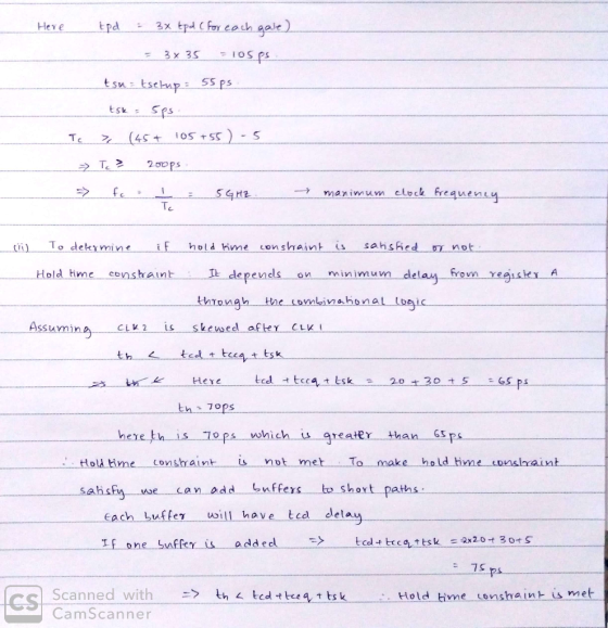
Given the register/combinational logic circuitry below, determine if the setup time constraint and hold time constraint...
(20 pts.) For the following circuit, the timing characteristics of the components are summarized below. .Flip-flop:...
 (20 pts.) For the following circuit, the timing characteristics of the components are summarized below. .Flip-flop: clock-to-Q maximum delay tpcq 40ps, clock-to-Q minimum delay tec 30ps, setup time tsetup 50ps, hold time thold 60ps Logic gate (each AND, OR, Inverter): propagation delay tpd 35ps, contamination delay ted25ps. FFl Fr3 CLK OUT FF2 CLK Suppose that there is no clock skew. What is the maximum clock frequency of this a. circuit? b. How much clock skew can the circuit tolerate before...
(b) Using a timing diagram showing the clk, Q1 and D2 signals, explain the following timing const...
 (b) Using a timing diagram showing the clk, Q1 and D2 signals, explain the following timing constraints for the circuit shown in Figure 2.1 cqtcd 2 old where tod is the contamination delay of the combinational logic 7 marks reg2 reg1 Combinational D2 logic clk. clk Figure 2.1 (c) In the circuit shown in Figure 2.2, the flip-flops have a clock-to-Q contamination delay of 30 ps and a propagation delay of 80 ps. They have a setup time of 50...
Suppose you have a synchronous sequential circuit whose clock has a cycle time of 900 ps...
 Suppose you have a synchronous sequential circuit whose clock has a cycle time of 900 ps (i.e., Te = 900 ps). The flip-flops have the timing characteristics given in Table 1 below. What is the minimum contamination delay of a combinational circuit between two registers? Give your answer in number of picoseconds (ps). For example, if your answer were 800 ps, you would write 800. Table 1. Flip-flop Timing Characteristics Timing characteristic toca Amount (in ps) 100 сса setup thold
3. (16 pts.) A sequential circuit design is shown in the following diagram CLK CLK Frt Trl Frl FF1 D-FF clk-to-q propagation delay tpcq 15 ps D-FF clk-to-q contamination delay tccq-10 ps D-FF dat...
 3. (16 pts.) A sequential circuit design is shown in the following diagram CLK CLK Frt Trl Frl FF1 D-FF clk-to-q propagation delay tpcq 15 ps D-FF clk-to-q contamination delay tccq-10 ps D-FF data setup time ts-15 ps D-FF data hold time th = 10 ps Gate 2-input NAND 2-input NOR 2-input XOIR NOT Tpd(ps) Tea(ps) 15 25 35 10 10 15 25 (8 pts.) Calculate the maximum clock frequency for reliable operation assuming there is no clock skew (8...
Timing Analysis of Combinational Logic Networks (b) Consider the combinational network shown below and use the...
 Timing Analysis of Combinational Logic Networks
(b) Consider the combinational network shown below and use the table of timing parameters to answer this question. Gate NAND2 NAND3 NOR2 AND2 Epa (PS203030 30 Icda (ps 15 25 25 25 i. What are the slow delay path(s) of the network? F Compute the network's overall propagation delay. What are the fast delay path(s)? Compute the network's overall contamination delay. ii.
Timing Analysis of Combinational Logic Networks
(b) Consider the combinational network shown below and use the table of timing parameters to answer this question. Gate NAND2 NAND3 NOR2 AND2 Epa (PS203030 30 Icda (ps 15 25 25 25 i. What are the slow delay path(s) of the network? F Compute the network's overall propagation delay. What are the fast delay path(s)? Compute the network's overall contamination delay. ii.
Name: (4) (10 pts) Design a Moore FSM that has one input A and one output Y, and the output Y should be 1 if A has...
 Name: (4) (10 pts) Design a Moore FSM that has one input A and one output Y, and the output Y should be 1 if A has been 101 during the most recent three consecutive clock cycles or A has been 1 during the two most recent consecutive clock cycles. You only need to write down your state transition diagram. (5) (6 pts) Consider the following sequential circuit. Each two-input OR gate has a propagation delay of 130ps and a...
2. A four-bit addition machine is built with four full adders such that the carry out...
 2. A four-bit addition machine is built with four full adders
such that the carry out of the first adder is the carry in to the
second adder, and the carry out of the second is the carry in to
the third, and so on as shown in Figure 2.
The machine has input and output registers and must complete the
addition in one clock cycle.
Each full adder has the following propagation delays: 20 ps from
Cin to Cout...
2. A four-bit addition machine is built with four full adders
such that the carry out of the first adder is the carry in to the
second adder, and the carry out of the second is the carry in to
the third, and so on as shown in Figure 2.
The machine has input and output registers and must complete the
addition in one clock cycle.
Each full adder has the following propagation delays: 20 ps from
Cin to Cout...
• In the circuit below, each register has a clock-to-Q propagation delay of 0.3ns and a...
 • In the circuit below, each register has a clock-to-Q propagation delay of 0.3ns and a setup time of 0.2ns. The rectangles at either end of the diagram are D Flip Flops. What is the max frequency of a 1 stage pipeline? 2 stage pipeline (most efficient)? 3 stage pipeline? SHOW YOUR WORK. Tc tpca + tpd + tsetup D Q CL 3.7ns CL 3.5ns CL 4.5ns D CL 4.7ns CL 4.3ns
Purpose The purpose of this homework is to better understand how real-world device delays effect the...
 Purpose The purpose of this homework is to better understand how real-world device delays effect the maximum speed of operation in sequential synchronous designs. Assignment A sequential network has been implemented using two D flip/flops, and discrete combinational logic as shown in the figure below. Assume that the inputs A and B always change at the same time as the falling edge of the 50% duty cycle clock. Also assume the following delay parameters for the combinational logic elements: The...
Design an electronic lock system. This system has 2 inputs: A and B. This system will...
 Design an electronic lock system. This system has 2 inputs: A and B. This system will be unlocked when the sequence BBA is pressed. State diagram of this electronic lock system is shown below. - Draw a circuit diagram and find the maximum clock frequency of your circuit. Check if this circuit violates any hold time violation Note: 1) This circuit is a Moore machine 2) Please assign each state as follows, XO = 00, x1 = 01, X2 =...
 (20 pts.) For the following circuit, the timing characteristics of the components are summarized below. .Flip-flop: clock-to-Q maximum delay tpcq 40ps, clock-to-Q minimum delay tec 30ps, setup time tsetup 50ps, hold time thold 60ps Logic gate (each AND, OR, Inverter): propagation delay tpd 35ps, contamination delay ted25ps. FFl Fr3 CLK OUT FF2 CLK Suppose that there is no clock skew. What is the maximum clock frequency of this a. circuit? b. How much clock skew can the circuit tolerate before...
 (b) Using a timing diagram showing the clk, Q1 and D2 signals, explain the following timing constraints for the circuit shown in Figure 2.1 cqtcd 2 old where tod is the contamination delay of the combinational logic 7 marks reg2 reg1 Combinational D2 logic clk. clk Figure 2.1 (c) In the circuit shown in Figure 2.2, the flip-flops have a clock-to-Q contamination delay of 30 ps and a propagation delay of 80 ps. They have a setup time of 50...
 Suppose you have a synchronous sequential circuit whose clock has a cycle time of 900 ps (i.e., Te = 900 ps). The flip-flops have the timing characteristics given in Table 1 below. What is the minimum contamination delay of a combinational circuit between two registers? Give your answer in number of picoseconds (ps). For example, if your answer were 800 ps, you would write 800. Table 1. Flip-flop Timing Characteristics Timing characteristic toca Amount (in ps) 100 сса setup thold
 3. (16 pts.) A sequential circuit design is shown in the following diagram CLK CLK Frt Trl Frl FF1 D-FF clk-to-q propagation delay tpcq 15 ps D-FF clk-to-q contamination delay tccq-10 ps D-FF data setup time ts-15 ps D-FF data hold time th = 10 ps Gate 2-input NAND 2-input NOR 2-input XOIR NOT Tpd(ps) Tea(ps) 15 25 35 10 10 15 25 (8 pts.) Calculate the maximum clock frequency for reliable operation assuming there is no clock skew (8...
 Timing Analysis of Combinational Logic Networks
(b) Consider the combinational network shown below and use the table of timing parameters to answer this question. Gate NAND2 NAND3 NOR2 AND2 Epa (PS203030 30 Icda (ps 15 25 25 25 i. What are the slow delay path(s) of the network? F Compute the network's overall propagation delay. What are the fast delay path(s)? Compute the network's overall contamination delay. ii.
Timing Analysis of Combinational Logic Networks
(b) Consider the combinational network shown below and use the table of timing parameters to answer this question. Gate NAND2 NAND3 NOR2 AND2 Epa (PS203030 30 Icda (ps 15 25 25 25 i. What are the slow delay path(s) of the network? F Compute the network's overall propagation delay. What are the fast delay path(s)? Compute the network's overall contamination delay. ii.
 Name: (4) (10 pts) Design a Moore FSM that has one input A and one output Y, and the output Y should be 1 if A has been 101 during the most recent three consecutive clock cycles or A has been 1 during the two most recent consecutive clock cycles. You only need to write down your state transition diagram. (5) (6 pts) Consider the following sequential circuit. Each two-input OR gate has a propagation delay of 130ps and a...
 2. A four-bit addition machine is built with four full adders
such that the carry out of the first adder is the carry in to the
second adder, and the carry out of the second is the carry in to
the third, and so on as shown in Figure 2.
The machine has input and output registers and must complete the
addition in one clock cycle.
Each full adder has the following propagation delays: 20 ps from
Cin to Cout...
2. A four-bit addition machine is built with four full adders
such that the carry out of the first adder is the carry in to the
second adder, and the carry out of the second is the carry in to
the third, and so on as shown in Figure 2.
The machine has input and output registers and must complete the
addition in one clock cycle.
Each full adder has the following propagation delays: 20 ps from
Cin to Cout...
 • In the circuit below, each register has a clock-to-Q propagation delay of 0.3ns and a setup time of 0.2ns. The rectangles at either end of the diagram are D Flip Flops. What is the max frequency of a 1 stage pipeline? 2 stage pipeline (most efficient)? 3 stage pipeline? SHOW YOUR WORK. Tc tpca + tpd + tsetup D Q CL 3.7ns CL 3.5ns CL 4.5ns D CL 4.7ns CL 4.3ns
 Purpose The purpose of this homework is to better understand how real-world device delays effect the maximum speed of operation in sequential synchronous designs. Assignment A sequential network has been implemented using two D flip/flops, and discrete combinational logic as shown in the figure below. Assume that the inputs A and B always change at the same time as the falling edge of the 50% duty cycle clock. Also assume the following delay parameters for the combinational logic elements: The...
 Design an electronic lock system. This system has 2 inputs: A and B. This system will be unlocked when the sequence BBA is pressed. State diagram of this electronic lock system is shown below. - Draw a circuit diagram and find the maximum clock frequency of your circuit. Check if this circuit violates any hold time violation Note: 1) This circuit is a Moore machine 2) Please assign each state as follows, XO = 00, x1 = 01, X2 =...
Most questions answered within 3 hours.
-
Suppose that XX is a random variable with mean 16 and standard
deviation 5 . Also...
asked 7 minutes ago -
Calculate the number density of argon gas at a temperature of
24C and a pressure of...
asked 3 hours ago -
Alternative
Classification
How to Estimate
Probabilities from Data? ( For continuous Attributes)
And How to generate...
asked 3 hours ago -
An explosion breaks a 20.0-kg object into three parts. The
object is initially moving at a...
asked 4 hours ago -
Calculate the approximate number of residues of Rubisco, which
is involved in carbon fixation in plants,...
asked 5 hours ago -
Other decisions about scientific claims can have a much broader
impact.ENERGYarrow-10x10.png, environment, health, security - all...
asked 6 hours ago -
I need to write a research paper and work cited about this
topic: The United States...
asked 6 hours ago -
Hello! I was wondering if I could have some help?
If the vapor pressure of carvone...
asked 6 hours ago -
An economist wants to estimate the mean per capita income (in
thousands of dollars) for a...
asked 7 hours ago -
What would be the input/output characteristic of a circuit
obtained by putting two of your 2's-complementers...
asked 7 hours ago -
In Drosophila, the transition from the syncytial blastoderm
stage to the cellular blastoderm stage is a...
asked 7 hours ago -
Project management question:
Name 3 different types of resources (hint: humans are one
type)
asked 7 hours ago