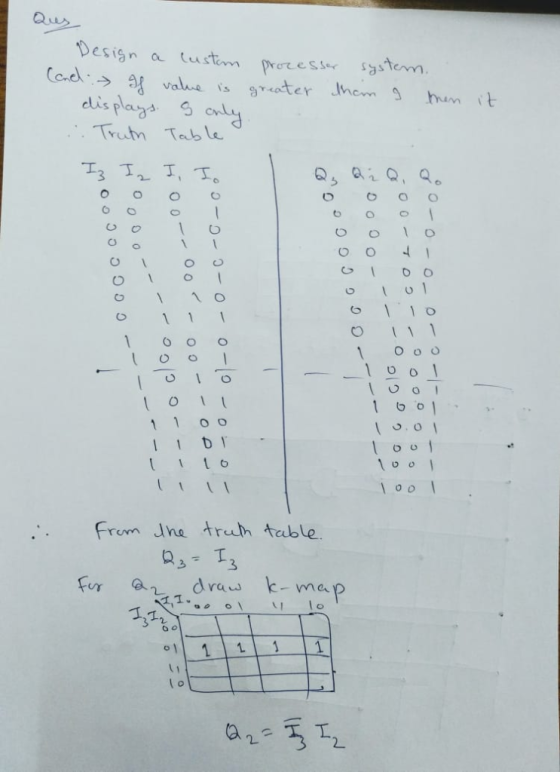
Design a custom processor system that displays (in 4-bit output Q) the last inputed 4-bit value A. If the 4-bit value is...
Design a custom processor system that displays (in 4-bit output Q) the last inputed 4-bit value A. If the 4-bit value is greater than 9 the processor rounds it off to 9 and diplays 9 (1001) instead.
Homework Answers

Add Answer to:
Design a custom processor system that displays (in 4-bit output Q) the last inputed 4-bit value A. If the 4-bit value is...
Design a sequential system that has one synchronous input bit stream x and one output z, with the following functionality and also follows the design constrains. Design Specifications: Design a sequen...
 Design a sequential system
that has one synchronous input bit stream x and one output z, with
the following functionality and also follows the design
constrains.
Design Specifications: Design a sequential system that has one synchronous input bit stream X and one output Z, with the following functionality 1) We look at every fourth-input-bit, while the other input bits are "don't cares". when three "consecutives" fourth-bits form the sequences 110 or 000 the system should output Z = 1, meaning...
Design a sequential system
that has one synchronous input bit stream x and one output z, with
the following functionality and also follows the design
constrains.
Design Specifications: Design a sequential system that has one synchronous input bit stream X and one output Z, with the following functionality 1) We look at every fourth-input-bit, while the other input bits are "don't cares". when three "consecutives" fourth-bits form the sequences 110 or 000 the system should output Z = 1, meaning...
A seven segment decoder is a digital circuit that displays an input value 0 through 9 as a digital output in the 7-segment display. The behavior of this design can be modeled with the schematic diagra...
 A seven segment decoder is a digital circuit that
displays an input value 0 through 9 as a digital output in the
7-segment display. The behavior of this design can be modeled with
the schematic diagram below, where DCBA is the 4-bit input (D is
the most significant bit and A is the least significant bit) and
abcdefg is the 7-segment output.
2. (20 POINTS) A seven segment decoder is a digital circuit that displays an input value 0 through...
A seven segment decoder is a digital circuit that
displays an input value 0 through 9 as a digital output in the
7-segment display. The behavior of this design can be modeled with
the schematic diagram below, where DCBA is the 4-bit input (D is
the most significant bit and A is the least significant bit) and
abcdefg is the 7-segment output.
2. (20 POINTS) A seven segment decoder is a digital circuit that displays an input value 0 through...
1. Cache memory (8pts) Consider adding cache to a processor-memory system design. The microprocessor without cache needs 12 clock cycles to read a 16-bit word from the memory. With cache, it take...
 1. Cache memory (8pts) Consider adding cache to a processor-memory system design. The microprocessor without cache needs 12 clock cycles to read a 16-bit word from the memory. With cache, it takes only 4 clock cycles if the data happens to be in the cache and a total 20 clock cycles including the cache misses. a. What is the performance ratio of the cache system to the non-cache system given a hit rate of 80%? b. For what hit rate...
1. Cache memory (8pts) Consider adding cache to a processor-memory system desigrn. The microprocessor without cache needs 12 clock cycles to read a 16-bit word from the memory. With cache, it takes o...
 1. Cache memory (8pts) Consider adding cache to a processor-memory system desigrn. The microprocessor without cache needs 12 clock cycles to read a 16-bit word from the memory. With cache, it takes only 4 clock cycles if the data happens to be in the cache and a total 20 clock cycles including the cache misses a. What is the performance ratio of the cache system to the non-cache system given a hit rate of 80%? b. For what hit rate...
3. (6 pts) Consider a new processor. The memory system is 32-bit byte- addressable. The on-chip...
 3. (6 pts) Consider a new processor. The memory system is 32-bit byte- addressable. The on-chip cache memory is 128 KByte 4-way set-associative, with a 64 byte block size. (a) Draw a diagram showing how the cache controller will split the memory address: for each field. show its name and number of bits. (b) The design team decided to change the cache architecture to a direct mapped one. For each of the parameters in the following table, indicate the impact...
Design a decoder that converts unsigned 4-bit binary numbers to codes for displaying the decimal value...
Design a decoder that converts unsigned 4-bit binary numbers to codes for displaying the decimal value of the binary number on two seven-segment displays. Leading zeros should be displayed as a blank display.
Design a combinational logic circuit which has one output Z and a 4-bit input ABCD representing...
Design a combinational logic circuit which has one output Z and a 4-bit input ABCD representing a binary number. Z should be 1 iff the input is at least 5, but is no greater than 11. Use one OR gate (three inputs) and three AND gates (with no more than three inputs each). Using K-map, find min SOP and min POS form for the outputs W, X
1. Design a combinational circuit that coverts a 4-bit Gray code to a 4-bit Excess-3 code....
 1. Design a combinational circuit that coverts a 4-bit Gray code to a 4-bit Excess-3 code. Provide detailed solution and explanation 2. Design a double edge-triggered D flip-flop using multiplexers only. The output of the flip-flop Q should "sample" the value of the input D on both rising (+ve) and falling -ve) edges of the clock CLK. Provide detailed solution and explanation 3. Design an FSM counter that counts the sequence: 00, 11, 01, 10, 00, 11, Provide detailed solution...
Design a combinational circuit that compares two 4-bit unsigned numbers A and B to see whether...
Design a combinational circuit that compares two 4-bit unsigned numbers A and B to see whether A is greater than B. The circuit has one output X, so that X = 0 if A ≤ B and X = 1 if A > B.
Design a computer system with an 8-bit address bus, an 8-bit data bus and it uses...
 Design a computer system with an 8-bit address bus, an 8-bit data bus and it uses isolated I/O. It has: 1128 bytes of PROM starting at address 00H (H meaning in hexadecimal) constructed usin ( one 64x8 chip and multiple 32x2 chips; g (2) 96 bytes of RAM constructed 32x4 chips; (3) an output device with a READY signal at address ABH; (4) an input device with a READY signal at address CDH; (5) a bidirectional input/output device with a...
 Design a sequential system
that has one synchronous input bit stream x and one output z, with
the following functionality and also follows the design
constrains.
Design Specifications: Design a sequential system that has one synchronous input bit stream X and one output Z, with the following functionality 1) We look at every fourth-input-bit, while the other input bits are "don't cares". when three "consecutives" fourth-bits form the sequences 110 or 000 the system should output Z = 1, meaning...
Design a sequential system
that has one synchronous input bit stream x and one output z, with
the following functionality and also follows the design
constrains.
Design Specifications: Design a sequential system that has one synchronous input bit stream X and one output Z, with the following functionality 1) We look at every fourth-input-bit, while the other input bits are "don't cares". when three "consecutives" fourth-bits form the sequences 110 or 000 the system should output Z = 1, meaning...
 A seven segment decoder is a digital circuit that
displays an input value 0 through 9 as a digital output in the
7-segment display. The behavior of this design can be modeled with
the schematic diagram below, where DCBA is the 4-bit input (D is
the most significant bit and A is the least significant bit) and
abcdefg is the 7-segment output.
2. (20 POINTS) A seven segment decoder is a digital circuit that displays an input value 0 through...
A seven segment decoder is a digital circuit that
displays an input value 0 through 9 as a digital output in the
7-segment display. The behavior of this design can be modeled with
the schematic diagram below, where DCBA is the 4-bit input (D is
the most significant bit and A is the least significant bit) and
abcdefg is the 7-segment output.
2. (20 POINTS) A seven segment decoder is a digital circuit that displays an input value 0 through...
 1. Cache memory (8pts) Consider adding cache to a processor-memory system design. The microprocessor without cache needs 12 clock cycles to read a 16-bit word from the memory. With cache, it takes only 4 clock cycles if the data happens to be in the cache and a total 20 clock cycles including the cache misses. a. What is the performance ratio of the cache system to the non-cache system given a hit rate of 80%? b. For what hit rate...
 1. Cache memory (8pts) Consider adding cache to a processor-memory system desigrn. The microprocessor without cache needs 12 clock cycles to read a 16-bit word from the memory. With cache, it takes only 4 clock cycles if the data happens to be in the cache and a total 20 clock cycles including the cache misses a. What is the performance ratio of the cache system to the non-cache system given a hit rate of 80%? b. For what hit rate...
 3. (6 pts) Consider a new processor. The memory system is 32-bit byte- addressable. The on-chip cache memory is 128 KByte 4-way set-associative, with a 64 byte block size. (a) Draw a diagram showing how the cache controller will split the memory address: for each field. show its name and number of bits. (b) The design team decided to change the cache architecture to a direct mapped one. For each of the parameters in the following table, indicate the impact...
 1. Design a combinational circuit that coverts a 4-bit Gray code to a 4-bit Excess-3 code. Provide detailed solution and explanation 2. Design a double edge-triggered D flip-flop using multiplexers only. The output of the flip-flop Q should "sample" the value of the input D on both rising (+ve) and falling -ve) edges of the clock CLK. Provide detailed solution and explanation 3. Design an FSM counter that counts the sequence: 00, 11, 01, 10, 00, 11, Provide detailed solution...
 Design a computer system with an 8-bit address bus, an 8-bit data bus and it uses isolated I/O. It has: 1128 bytes of PROM starting at address 00H (H meaning in hexadecimal) constructed usin ( one 64x8 chip and multiple 32x2 chips; g (2) 96 bytes of RAM constructed 32x4 chips; (3) an output device with a READY signal at address ABH; (4) an input device with a READY signal at address CDH; (5) a bidirectional input/output device with a...
Most questions answered within 3 hours.
-
10. Complete the table below
only using hexadecimal numbers:
AL CODE
EBX
EAX
[EAX]
mov eax,...
asked 3 minutes ago -
trust is best established through the combination of ------and
------- .
1. magnanimity and justice
2....
asked 18 minutes ago -
Blood pressure is normally taken on the upper arm at the level
of the heart. Suppose,...
asked 16 minutes ago -
Suppose that the satellite around the earth has an orbit that is
24 KM larger in...
asked 20 minutes ago -
Calculate the [OH (aq)] in limes which have a [H3O*(aq)] of 1.3 x
10 mol/L
asked 18 minutes ago -
A nozzle with a radius of 0.250 cm is attached to a garden hose
with a...
asked 29 minutes ago -
PLEASE do not use any loops for the program; only recursion is
allowed
4. Write a...
asked 38 minutes ago -
Please help me with me. I did the first part to write the operations but in...
asked 35 minutes ago -
Use Cryptool to find the Cryptographic SHA-1 hash value of the
string "abc". The calculator is...
asked 39 minutes ago -
You are attempting to calculate a firm’s free cash flow to
equity. You know the following...
asked 1 hour ago -
the following reaction occurs in a balloon containing
N2O2 gas
N2O4(g)=2NO2(g)
will the volume of the...
asked 2 hours ago -
answer the questions throughout this program
public class Day implements Comparable {
Private Boolean atWork;...
asked 2 hours ago