

Now remove the negative voltage supply (V2) and connect the supply directly to ground as shown in e. Figure 2. Change the amplitude of the input voltage (V3) back to 1 V ww 3k9 VI SV U1 PRI ww V3 RL k9 1V 1k2 1kHz 0 0 Figure 2 f. Simulate the circuit and determine the following values. (7) Maximum voltage at the output node (PR2): VPR2, max VPR2, mine (8) Approximate minimum voltage at the output node (PR2):
Homework Answers
Add Answer to:
Procedure Load Multisim Live in a web browser and sign in. Create a new circuit. a....
Procedure Load Multisim Live in a web browser and sign in. Create a new circuit. a....
 Procedure Load Multisim Live in a web browser and sign in. Create a new circuit. a. Place the components and wire up the circuit shown in Figure 1 b. D1 D2 R1 V1 2k9 10V Figure 1 Set the simulation mode to "DC Op". Simulate the circuit and determine the following values C. (1) Voltage at node 2: V= (2) Voltage at node 3: V3 Total current (3) Change the resistor value to 50. Answer the following questions. d. (4)...
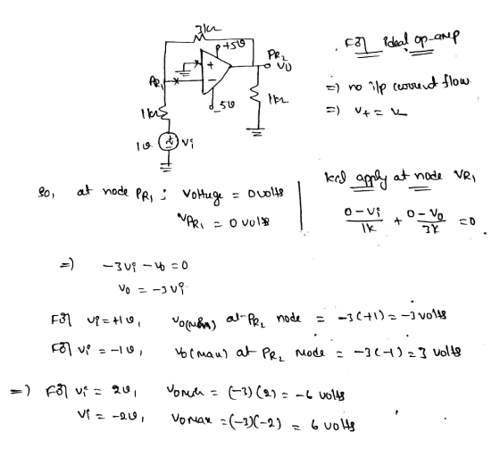
Assuming an ideal op-amp in the following circuit, find output voltage, Vo if R1= 2 K2,...
 Assuming an ideal op-amp in the following circuit, find output voltage, Vo if R1= 2 K2, R2=8 K2, R3=5.1 K2, R4=6 KN, R5=14 KN, R6=4.2 KS, RL=10.3 KS, V1=1V, 12=0.5 mA and V3=3.2 V. R6 R1 R5 Vo w + * RL + 12 R2 V1 R3 R4 V3 Answer: OV Using the above circuit, but consider the following component values: R1= 2 K12 R2=8 K2, R3=2.9 K2, R4=6 KI2, R5=10.8 K92, R6=15 KO, RL=10 K2, V1=1V, 12=0.5mA and V3=2V....
Assuming an ideal op-amp in the following circuit, find output voltage, Vo if R1= 2 K12,...
 Assuming an ideal op-amp in the following circuit, find output voltage, Vo if R1= 2 K12, R2=8 KN, R3=3.9 KN, R4=6 KN, R5=18 K2, R6=4.4 KN, RL=12.5 KN, V1=1V, 12=0.5 mA and V3=3.4 V. R6 R1 R5 Vo + + RL R2 V1 R3 R4 + V3 Answer: LOV Using the above circuit, but consider the following component values: R1= 2 KO2 R2=8 K12, R3=3.6 K12, R4=6 K12, R5=16.9 KN, R6=15 KN, RL=10 KO, V1=1V, 12=0.5mA and V3=2V. What is...
Assuming an ideal op-amp in the following circuit, find output voltage, Vo if R1= 2 K2,...
 Assuming an ideal op-amp in the following circuit, find output voltage, Vo if R1= 2 K2, R2=8 K12, R3=3.8 KS2, R4=6 KI2, R5=15 KS2, R6=3.8 KN, RL=9.8 K12, V1=1V, 12=0.5 mA and V3=2.2 V. } R6 R1 w R5 w + Vo + } RL 12 R2 V1 R3 R4 + +1 V3 Using the above circuit, but consider the following component values: R1= 2 KN R2=8 K2, R3=4.1 K12, R4=6 KI2, R5=17.0 K12, R6=15 KI, RL=10 KI, V1=1V, 12=0.5mA...
Score 2. (22 points) For the circuit in Figure 2, the transistor parameters are: 2 0,...
 Score 2. (22 points) For the circuit in Figure 2, the transistor parameters are: 2 0, VN=2V, Ka-1mA/V2, all the capacitors are assumed to act as short circuits at the signal frequency (1) Calculate the Q-point (Vos. I Vos); (2) Sketch the small-signal equivalent circuit, you must label the polarities of the voltages and the direction of the current; (3) Determine the voltage gain A, vo/v (4) Determine the input resistance Ri and output resistance Ro V1 5 10 V...
3 Circuit C2 R1 Connect to Vo Unity Gair 470 0.1uF Follower Ground Output C1 4700 R2 R3 1000 C3 luF Figure 1. AC Test C...
 3 Circuit C2 R1 Connect to Vo Unity Gair 470 0.1uF Follower Ground Output C1 4700 R2 R3 1000 C3 luF Figure 1. AC Test Circuit. 5 LTspice Simulation » Use LTspice to simulate the circuit shown in Figure 1. . The AC voltage source should have an amplitude of 5V and a frequency of 60Hz. When you enter the parameters in LTspice, you should see them displayed on the schematic as follows SINE(0 5 60000 1000) * Graph the...
1. Use MultiSim program to simulate the RC circuit shown in Figures 1 using nominal resistor valu...
 1. Use MultiSim program to simulate the RC circuit shown in Figures 1 using nominal resistor value of 100Ω and 10uF capacitor. Set up the function generator for: square wave, frequency 20Hz, duty cycle 50%, offset 1V, and amplitude 1V. Use Tektronix scope to display the input source and the capacitor voltage waveforms on the same display 2. Print out your schematics and print an output showing Channels A and B 3. Use the scope cursors to measure simulated t...
w A ovo 3. (15 pts) The input Vg to the rectifier circuit on the right...
 w A ovo 3. (15 pts) The input Vg to the rectifier circuit on the right is a sinusoidal signal of amplitude 4V, as shown below. Use the 0.7V voltage drop model for the diode. a) Determine the maximum and minimum values of the output voltage V across load resistor RL. b) Determine the conduction angle. c) Determine the percent conduction. 10022 {RL 2002 3. (15 pts) The input to the rectifier circuit on the right is sinusoidal signal of...
Lab - 4.pdf (page 1 of 2) @ Search R2 Prelab Resistor Selection R1 w a....
 Lab - 4.pdf (page 1 of 2) @ Search R2 Prelab Resistor Selection R1 w a. A circuit based on the configuration in Figure 1 1 ΚΩ needs to produce: V2 R3 V1 1) A leftward current of 3.9 mA in R5. V3 2) A top-positive voltage of 1.5 V across R4. 3) A power of 2.4 mW in RL. 4.0V R4 RL = 5602 b. Sketch Figure 1 on a blank sheet of paper, add notations as needed, and...
To design a high efficiency d.c., to d.c power converter with the given specifications min 10V max 15V nominal (regulated) 8V Input voltage: Output voltage: Nominal load current: 4A Inductor current...
 To design a high efficiency d.c., to d.c power converter with the given specifications min 10V max 15V nominal (regulated) 8V Input voltage: Output voltage: Nominal load current: 4A Inductor current ripple: 0.1A max Switching frequency: 30 kHz Output voltage ripple: 20 mV Define a suitable power circuit topology to meet the above specification? Sketch a circuit diagram of the chosen power circuit topology (a) Define the minimum and maximum duty cycles assuming that the control circuit keeps the output...
 Procedure Load Multisim Live in a web browser and sign in. Create a new circuit. a. Place the components and wire up the circuit shown in Figure 1 b. D1 D2 R1 V1 2k9 10V Figure 1 Set the simulation mode to "DC Op". Simulate the circuit and determine the following values C. (1) Voltage at node 2: V= (2) Voltage at node 3: V3 Total current (3) Change the resistor value to 50. Answer the following questions. d. (4)...
 Assuming an ideal op-amp in the following circuit, find output voltage, Vo if R1= 2 K2, R2=8 K2, R3=5.1 K2, R4=6 KN, R5=14 KN, R6=4.2 KS, RL=10.3 KS, V1=1V, 12=0.5 mA and V3=3.2 V. R6 R1 R5 Vo w + * RL + 12 R2 V1 R3 R4 V3 Answer: OV Using the above circuit, but consider the following component values: R1= 2 K12 R2=8 K2, R3=2.9 K2, R4=6 KI2, R5=10.8 K92, R6=15 KO, RL=10 K2, V1=1V, 12=0.5mA and V3=2V....
 Assuming an ideal op-amp in the following circuit, find output voltage, Vo if R1= 2 K12, R2=8 KN, R3=3.9 KN, R4=6 KN, R5=18 K2, R6=4.4 KN, RL=12.5 KN, V1=1V, 12=0.5 mA and V3=3.4 V. R6 R1 R5 Vo + + RL R2 V1 R3 R4 + V3 Answer: LOV Using the above circuit, but consider the following component values: R1= 2 KO2 R2=8 K12, R3=3.6 K12, R4=6 K12, R5=16.9 KN, R6=15 KN, RL=10 KO, V1=1V, 12=0.5mA and V3=2V. What is...
 Assuming an ideal op-amp in the following circuit, find output voltage, Vo if R1= 2 K2, R2=8 K12, R3=3.8 KS2, R4=6 KI2, R5=15 KS2, R6=3.8 KN, RL=9.8 K12, V1=1V, 12=0.5 mA and V3=2.2 V. } R6 R1 w R5 w + Vo + } RL 12 R2 V1 R3 R4 + +1 V3 Using the above circuit, but consider the following component values: R1= 2 KN R2=8 K2, R3=4.1 K12, R4=6 KI2, R5=17.0 K12, R6=15 KI, RL=10 KI, V1=1V, 12=0.5mA...
 Score 2. (22 points) For the circuit in Figure 2, the transistor parameters are: 2 0, VN=2V, Ka-1mA/V2, all the capacitors are assumed to act as short circuits at the signal frequency (1) Calculate the Q-point (Vos. I Vos); (2) Sketch the small-signal equivalent circuit, you must label the polarities of the voltages and the direction of the current; (3) Determine the voltage gain A, vo/v (4) Determine the input resistance Ri and output resistance Ro V1 5 10 V...
 3 Circuit C2 R1 Connect to Vo Unity Gair 470 0.1uF Follower Ground Output C1 4700 R2 R3 1000 C3 luF Figure 1. AC Test Circuit. 5 LTspice Simulation » Use LTspice to simulate the circuit shown in Figure 1. . The AC voltage source should have an amplitude of 5V and a frequency of 60Hz. When you enter the parameters in LTspice, you should see them displayed on the schematic as follows SINE(0 5 60000 1000) * Graph the...
 1. Use MultiSim program to simulate the RC circuit shown in Figures 1 using nominal resistor value of 100Ω and 10uF capacitor. Set up the function generator for: square wave, frequency 20Hz, duty cycle 50%, offset 1V, and amplitude 1V. Use Tektronix scope to display the input source and the capacitor voltage waveforms on the same display 2. Print out your schematics and print an output showing Channels A and B 3. Use the scope cursors to measure simulated t...
 w A ovo 3. (15 pts) The input Vg to the rectifier circuit on the right is a sinusoidal signal of amplitude 4V, as shown below. Use the 0.7V voltage drop model for the diode. a) Determine the maximum and minimum values of the output voltage V across load resistor RL. b) Determine the conduction angle. c) Determine the percent conduction. 10022 {RL 2002 3. (15 pts) The input to the rectifier circuit on the right is sinusoidal signal of...
 Lab - 4.pdf (page 1 of 2) @ Search R2 Prelab Resistor Selection R1 w a. A circuit based on the configuration in Figure 1 1 ΚΩ needs to produce: V2 R3 V1 1) A leftward current of 3.9 mA in R5. V3 2) A top-positive voltage of 1.5 V across R4. 3) A power of 2.4 mW in RL. 4.0V R4 RL = 5602 b. Sketch Figure 1 on a blank sheet of paper, add notations as needed, and...
 To design a high efficiency d.c., to d.c power converter with the given specifications min 10V max 15V nominal (regulated) 8V Input voltage: Output voltage: Nominal load current: 4A Inductor current ripple: 0.1A max Switching frequency: 30 kHz Output voltage ripple: 20 mV Define a suitable power circuit topology to meet the above specification? Sketch a circuit diagram of the chosen power circuit topology (a) Define the minimum and maximum duty cycles assuming that the control circuit keeps the output...
Most questions answered within 3 hours.
-
Please Help ASAP.
1Consider the below code which iterates over a linked
list of n nodes...
asked 12 minutes ago -
Determine the air to fuel ratio of:
Canadian natural gas, with 93.9% methane, 4.2% ethane, 0.3%...
asked 12 minutes ago -
A manufacturer of power tools claims that the average amount of
time required to assemble their...
asked 14 minutes ago -
"electron-withdrawing substituents on carbon encourage back
donation", then on the next page he says that "greater...
asked 26 minutes ago -
On December 31, 2016, the shareholders’ equity section of the
balance sheet of R & L...
asked 34 minutes ago -
16.7
At t=0s a small "upward" (positive y) pulse centered at x = 5.0
m is...
asked 47 minutes ago -
Twitter Users and News: A poll conducted in 2013 found that 52%
of U.S. adult Twitter...
asked 1 hour ago -
How
would I know whether a given amino acid has an ionizable group or
not? please...
asked 1 hour ago -
True or false?
True False The function of the enzyme acyl CoA
synthetase is the ATP-dependent coupling...
asked 1 hour ago -
Nadia Corporation adjusts its debt so that its interest coverage
(EBIT/Interest) remains constant at 3. Nadia’s...
asked 1 hour ago -
In a clinical trial, 20 out of 600 patients taking a
prescription drug complained of flulike...
asked 1 hour ago -
7. How many types of nuclear processes can produce energy? 8.
How many types of radioactive...
asked 1 hour ago