
Homework Answers

Add Answer to:
An NPN bipolar junction transistor (BJT) is used to turn on and off a 30 Ohm...
4. Lab VIII: Experiment VII The Bipolar Junction Transistor (BJT) Characteristics The bipolar junction transistor (BJT)...
 4. Lab VIII: Experiment VII The Bipolar Junction Transistor (BJT) Characteristics The bipolar junction transistor (BJT) is a three-terminal solid state device widely used as an amplifier (or switching) device. It consists of two n-type materials sandwiched by p-type material (npn) or two p-type and n-type. The terminals (sections) are known as emitter E, base B and collector C. Two currents and two voltages uniquely describe the behavior of the device. The third current/voltage can be determined through KCL/KVL. See...
Consider the npn BJT with a turn-on voltage V1 = 0.70 V, and a saturation emitter-collector...
 Consider the npn BJT with a turn-on voltage V1 = 0.70 V, and a saturation emitter-collector voltage V CE/SAT) = 0.20 V. (a) [20 points) Consider this transistor in a common- emitter circuit (Re = 0). Design this common- emitter circuit to produce the IV (Ic vs. VCE) characteristic and load line (LL) as shown in the graph. Your answers are the following: a drawing of the circuit; the values of Vcc, Rc, VBB, and Ra; and the value for...
ASAP! Question 1 [Soalan 1] (a) Describe the condition when a npn BJT transistor operates in...
 ASAP!
Question 1 [Soalan 1] (a) Describe the condition when a npn BJT transistor operates in saturation condition and what are the terminal currents and voltages conditions during saturation. [Terangkan keadaan bila satu transistor BJT npn beroperasi dalam keadaan tepu dan apakah keadaan arus dan voltan terminal semasa tepu. ] (20 Marks/Markah) (b) Consider the BJT transistor circuit in Figure 1. If Bpc = 100 and VBE = 0.65V, calculate: [Pertimbangkan litar transistor BJT dalam Rajah 1. Jika Bpc =...
ASAP!
Question 1 [Soalan 1] (a) Describe the condition when a npn BJT transistor operates in saturation condition and what are the terminal currents and voltages conditions during saturation. [Terangkan keadaan bila satu transistor BJT npn beroperasi dalam keadaan tepu dan apakah keadaan arus dan voltan terminal semasa tepu. ] (20 Marks/Markah) (b) Consider the BJT transistor circuit in Figure 1. If Bpc = 100 and VBE = 0.65V, calculate: [Pertimbangkan litar transistor BJT dalam Rajah 1. Jika Bpc =...
2. (15 pts) An npn bipolar junction transistor is biased in the forward-active region. The common-base...
 2. (15 pts) An npn bipolar junction transistor is biased in the forward-active region. The common-base current gain, α 0.95. The input emitter current is IE-4.6 mA. a) Calculate the collector current Ic b) Calculate the common-emitter current gain, B c) Calculate the base current IB IB
Problem 2. A silicon NPN bipolar transistor has the following specifications: Emitter: N+: ND =1018 cm-3...
Problem 2. A silicon NPN bipolar transistor has the following specifications: Emitter: N+: ND =1018 cm-3 , base: p-type, NA=1015 cm-3, collector: N-type, ND=5x1015 cm-3 . 1. Draw the energy band diagram of the transistor at thermal equilibrium, 2. If the transistor is biased at Normal Active Mode, emitter-base junction forward biased with 1 V, and collector-base junction is reverse biased with 4V, draw the energy band diagram.
question 3 and 4 Problem2 (30 points) Consider an npn bipolar transistor with the following characteristics...
 question 3 and 4
Problem2 (30 points) Consider an npn bipolar transistor with the following characteristics Base Collector Emitter Na-5x 1016 cm3 Ng- 1015 cm3 N1018 cm3 DC- 12 cm-/sec DE 8 cm-/sec (diff coef.) DB 15 cm-/sec sec TEO 108 sec (life time) tB0 5x 10 tCo 10 sec xp 0.7 um (Base width) xg 0.8 um (emitter width) D Remember D/u= KT /q, and L n.p n.p A forward bias of 0.5 V is applied to the emitter-base...
question 3 and 4
Problem2 (30 points) Consider an npn bipolar transistor with the following characteristics Base Collector Emitter Na-5x 1016 cm3 Ng- 1015 cm3 N1018 cm3 DC- 12 cm-/sec DE 8 cm-/sec (diff coef.) DB 15 cm-/sec sec TEO 108 sec (life time) tB0 5x 10 tCo 10 sec xp 0.7 um (Base width) xg 0.8 um (emitter width) D Remember D/u= KT /q, and L n.p n.p A forward bias of 0.5 V is applied to the emitter-base...
3. A silicon npn bipolar transistor is uniformly doped and biased in the forward active region wi...
 3. A silicon npn bipolar transistor is uniformly doped and biased in the forward active region with the base-collector junction reverse biased by 2.5 V. The metallurgical base width is 1.5 μm. The emitter, base collector doping concentrations are 5 × 10¹⁷, 1016, 2 × 1015 cm-3 respectively. a. At T-300 K, calculate the base-emitter voltage at which the minority carrier electron concentration at x-0 is 20% of the majority carrier hole concentration. At this voltage calculate the minority carrier...
*5. Design a BJT transistor drive circuit like the one shown Figure 10-7 (Hart's text) with an in...
 *5. Design a BJT transistor drive circuit like the one shown Figure 10-7 (Hart's text) with an initial peak base current, IB,-8 1B2, where 1B2 denotes the minimum base current required to drive the transistor to saturation. Assume a collector load resistance, Rc-8 Ω, collector supply voltage Vs = 30 V, large signal current of the transistor, hFE-min. 10, max. 20), VBE(on)-0.8 V, and the input is periodic pulse waveform (0 to 6) V, with a duty cycle, D-0.5. Also,...
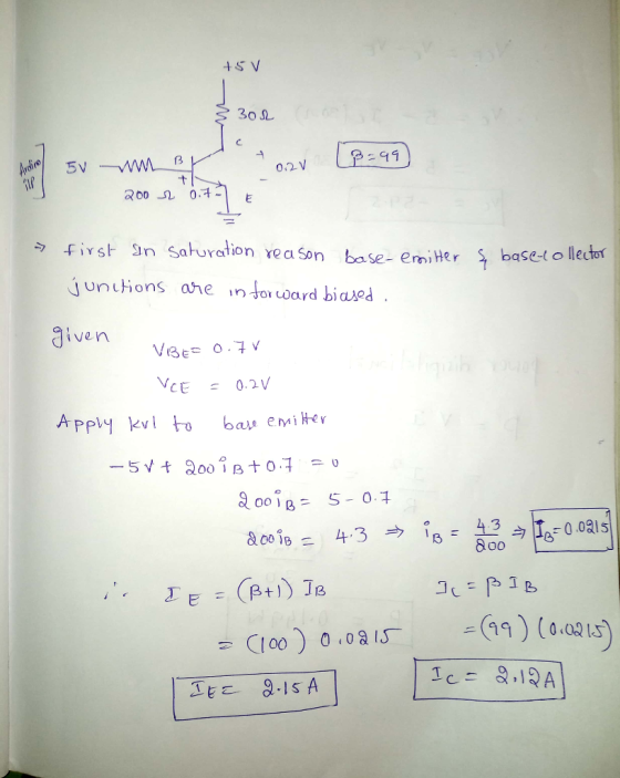
In the circuit shown, the motor can be modeled as a 30-ohm resistor. Determine the power...
 In the circuit shown, the motor can be modeled as a 30-ohm resistor. Determine the power delivered to the motor when the transistor is in the saturation mode. Assume the voltage drop across the collector-emitter junction of the transistor, V_CE, is 0.2 V. Insert a numeric answer in units of Watts. +6 loor CV - B
*5. Design a BJT transistor drive circuit like the one shown Figure 10-7 (Hart's text) with...
 *5. Design a BJT transistor drive circuit like the one shown Figure 10-7 (Hart's text) with an initial peak base current, IB,-8 1B2, where 1B2 denotes the minimum base current required to drive the transistor to saturation. Assume a collector load resistance, Rc-8 Ω, collector supply voltage Vs = 30 V, large signal current of the transistor, hFE-min. 10, max. 20), VBE(on)-0.8 V, and the input is periodic pulse waveform (0 to 6) V, with a duty cycle, D-0.5. Also,...
 4. Lab VIII: Experiment VII The Bipolar Junction Transistor (BJT) Characteristics The bipolar junction transistor (BJT) is a three-terminal solid state device widely used as an amplifier (or switching) device. It consists of two n-type materials sandwiched by p-type material (npn) or two p-type and n-type. The terminals (sections) are known as emitter E, base B and collector C. Two currents and two voltages uniquely describe the behavior of the device. The third current/voltage can be determined through KCL/KVL. See...
 Consider the npn BJT with a turn-on voltage V1 = 0.70 V, and a saturation emitter-collector voltage V CE/SAT) = 0.20 V. (a) [20 points) Consider this transistor in a common- emitter circuit (Re = 0). Design this common- emitter circuit to produce the IV (Ic vs. VCE) characteristic and load line (LL) as shown in the graph. Your answers are the following: a drawing of the circuit; the values of Vcc, Rc, VBB, and Ra; and the value for...
 ASAP!
Question 1 [Soalan 1] (a) Describe the condition when a npn BJT transistor operates in saturation condition and what are the terminal currents and voltages conditions during saturation. [Terangkan keadaan bila satu transistor BJT npn beroperasi dalam keadaan tepu dan apakah keadaan arus dan voltan terminal semasa tepu. ] (20 Marks/Markah) (b) Consider the BJT transistor circuit in Figure 1. If Bpc = 100 and VBE = 0.65V, calculate: [Pertimbangkan litar transistor BJT dalam Rajah 1. Jika Bpc =...
ASAP!
Question 1 [Soalan 1] (a) Describe the condition when a npn BJT transistor operates in saturation condition and what are the terminal currents and voltages conditions during saturation. [Terangkan keadaan bila satu transistor BJT npn beroperasi dalam keadaan tepu dan apakah keadaan arus dan voltan terminal semasa tepu. ] (20 Marks/Markah) (b) Consider the BJT transistor circuit in Figure 1. If Bpc = 100 and VBE = 0.65V, calculate: [Pertimbangkan litar transistor BJT dalam Rajah 1. Jika Bpc =...
 2. (15 pts) An npn bipolar junction transistor is biased in the forward-active region. The common-base current gain, α 0.95. The input emitter current is IE-4.6 mA. a) Calculate the collector current Ic b) Calculate the common-emitter current gain, B c) Calculate the base current IB IB
 question 3 and 4
Problem2 (30 points) Consider an npn bipolar transistor with the following characteristics Base Collector Emitter Na-5x 1016 cm3 Ng- 1015 cm3 N1018 cm3 DC- 12 cm-/sec DE 8 cm-/sec (diff coef.) DB 15 cm-/sec sec TEO 108 sec (life time) tB0 5x 10 tCo 10 sec xp 0.7 um (Base width) xg 0.8 um (emitter width) D Remember D/u= KT /q, and L n.p n.p A forward bias of 0.5 V is applied to the emitter-base...
question 3 and 4
Problem2 (30 points) Consider an npn bipolar transistor with the following characteristics Base Collector Emitter Na-5x 1016 cm3 Ng- 1015 cm3 N1018 cm3 DC- 12 cm-/sec DE 8 cm-/sec (diff coef.) DB 15 cm-/sec sec TEO 108 sec (life time) tB0 5x 10 tCo 10 sec xp 0.7 um (Base width) xg 0.8 um (emitter width) D Remember D/u= KT /q, and L n.p n.p A forward bias of 0.5 V is applied to the emitter-base...
 3. A silicon npn bipolar transistor is uniformly doped and biased in the forward active region with the base-collector junction reverse biased by 2.5 V. The metallurgical base width is 1.5 μm. The emitter, base collector doping concentrations are 5 × 10¹⁷, 1016, 2 × 1015 cm-3 respectively. a. At T-300 K, calculate the base-emitter voltage at which the minority carrier electron concentration at x-0 is 20% of the majority carrier hole concentration. At this voltage calculate the minority carrier...
 *5. Design a BJT transistor drive circuit like the one shown Figure 10-7 (Hart's text) with an initial peak base current, IB,-8 1B2, where 1B2 denotes the minimum base current required to drive the transistor to saturation. Assume a collector load resistance, Rc-8 Ω, collector supply voltage Vs = 30 V, large signal current of the transistor, hFE-min. 10, max. 20), VBE(on)-0.8 V, and the input is periodic pulse waveform (0 to 6) V, with a duty cycle, D-0.5. Also,...
 In the circuit shown, the motor can be modeled as a 30-ohm resistor. Determine the power delivered to the motor when the transistor is in the saturation mode. Assume the voltage drop across the collector-emitter junction of the transistor, V_CE, is 0.2 V. Insert a numeric answer in units of Watts. +6 loor CV - B
 *5. Design a BJT transistor drive circuit like the one shown Figure 10-7 (Hart's text) with an initial peak base current, IB,-8 1B2, where 1B2 denotes the minimum base current required to drive the transistor to saturation. Assume a collector load resistance, Rc-8 Ω, collector supply voltage Vs = 30 V, large signal current of the transistor, hFE-min. 10, max. 20), VBE(on)-0.8 V, and the input is periodic pulse waveform (0 to 6) V, with a duty cycle, D-0.5. Also,...
Most questions answered within 3 hours.
-
(Expected rate of return and risk) Carter Inc. is evaluating a
security. Calculate the investment’s expected...
asked 1 hour ago -
What specific indicators can point to lack of progress for
African Americans in American society?
asked 2 hours ago -
1-The Electrons in a beam are moving at 2.7×10⁸ m/s in an
electric field of 15000...
asked 3 hours ago -
A gas tank is a vertical cylinder. It has a radius of 1m, a
height of...
asked 3 hours ago -
Accent Software faces the following conditions. All of these
support Accent’s use of a market-penetration pricing...
asked 4 hours ago -
A mathematically inclined friend emails you the following
instructions: "Meet me in the cafeteria the first...
asked 4 hours ago -
A monopoly sells in two countries . The demand curves in the two
countries are p1...
asked 5 hours ago -
A .15kg rubber ball is bounced off a wall. Before hitting the
wall, the ball moves...
asked 6 hours ago -
A manufacturing company preparing to build a new plant is
considering three potential locations for it....
asked 6 hours ago -
B. If compound Y has approximately the same values of solubility
in toluene as compound X,...
asked 6 hours ago -
Oscar Inc. has inventory in Japan valued at 39,051,000 Yen one
year ago. One year ago...
asked 7 hours ago -
If Canada suffered from "fundamental disequilibrium," and its
government choose not to devalue its currency, a...
asked 7 hours ago