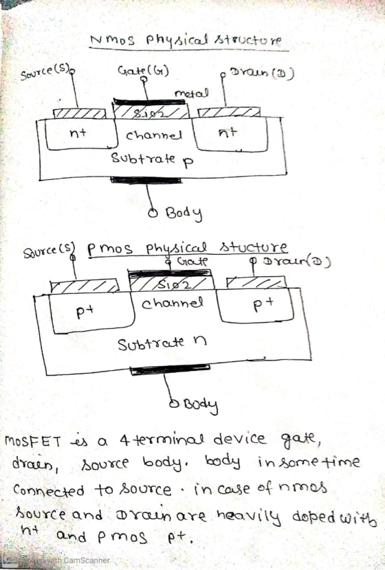
Physical structure of MOSFET (both NMOS and PMOS) Operation of MOSFET in cut-off, in triode and...
Physical structure of MOSFET (both NMOS and PMOS)
Operation of MOSFET in cut-off, in triode and in saturation mode
MOSFET as an amplifier
Please explain them.Thanks.
Homework Answers


Add Answer to:
Physical structure of MOSFET (both NMOS and PMOS)
Operation of MOSFET in cut-off, in triode and...
5. The NMOS and PMOS transistors in the below circuit are matched with kn’(Wn/Ln)=kp'(Wp/Lp)=1 mA/V2 and...
 5. The NMOS and PMOS transistors in the below circuit are matched with kn’(Wn/Ln)=kp'(Wp/Lp)=1 mA/V2 and Vin=-Vt=1V. (20 pts) +5 V a) Which MOSFET is cut-off, NMOS (QN) or PMOS (QP) for VF-5V? Why (5 pts) Qp -5 Vo Ipp Vo VION ON -5 V b) When VF-5V, in which mode, saturation or triode, the circuit operate? Explain why? (5 pts) c) Find the drain current ipy and ipp and the voltage vo for VF-5V (10 pts)
help me please subscription 5. The PMOS transistor has Vtp=-1 V. If the voltages of three...
 help me please
subscription 5. The PMOS transistor has Vtp=-1 V. If the voltages of three terminals are: Vg=2 V, Vs=5v, Vd=3.5V, then the transistor is operated in a) Cut off region b) Triode region c) Saturation region d) Unknown 6. The voltage transfer characteristic of a CMOS inverter is shown in Fig. 4. Threshold voltages Vrn = |Vpl = 0.5V. If Vpo=5V and the input v=3V, then Saved to this PC a) Both PMOS and NMOS in triode region...
help me please
subscription 5. The PMOS transistor has Vtp=-1 V. If the voltages of three terminals are: Vg=2 V, Vs=5v, Vd=3.5V, then the transistor is operated in a) Cut off region b) Triode region c) Saturation region d) Unknown 6. The voltage transfer characteristic of a CMOS inverter is shown in Fig. 4. Threshold voltages Vrn = |Vpl = 0.5V. If Vpo=5V and the input v=3V, then Saved to this PC a) Both PMOS and NMOS in triode region...
Triode region help. PMOS and NMOS . Saturation question. my work is below...did I do this...
 Triode region help. PMOS and NMOS . Saturation question. my work
is below...did I do this right? I feel I am missing something. Are
they both showing saturation?
In the following problems, unless otherwise stated, assume unCox = 200 u A/V, MpCox 100 u A/V, and Vth = 0.4 V for NMOS devices and —0.4 V for PMOS devices. 6.24. In the Fig. 6.42 , what is the minimum allow- able value of Vpp if M1 must not enter the...
Triode region help. PMOS and NMOS . Saturation question. my work
is below...did I do this right? I feel I am missing something. Are
they both showing saturation?
In the following problems, unless otherwise stated, assume unCox = 200 u A/V, MpCox 100 u A/V, and Vth = 0.4 V for NMOS devices and —0.4 V for PMOS devices. 6.24. In the Fig. 6.42 , what is the minimum allow- able value of Vpp if M1 must not enter the...
MOSFET design, KCL, KVL, nmos, pmos 40μΑ Qi. Consider the amplifier shown below. Assume the MOSFET...
 MOSFET design, KCL, KVL, nmos, pmos
40μΑ Qi. Consider the amplifier shown below. Assume the MOSFET has K,-- V. IV, Cg,-0.8pF, Cgdー0.2pF and no body effect. Given RB-100Rs, RREF the small signal AC gain is -1.6. 4kQand (a) Design RB and Rs so that the fu is 40MHz (b) Design CL so that the fi is 50Hz. 10V Mi RREF RB Rs M2 CL RD 1 00kΩ
MOSFET design, KCL, KVL, nmos, pmos
40μΑ Qi. Consider the amplifier shown below. Assume the MOSFET has K,-- V. IV, Cg,-0.8pF, Cgdー0.2pF and no body effect. Given RB-100Rs, RREF the small signal AC gain is -1.6. 4kQand (a) Design RB and Rs so that the fu is 40MHz (b) Design CL so that the fi is 50Hz. 10V Mi RREF RB Rs M2 CL RD 1 00kΩ
Label the source and drain... Vth = 0.4 for NMOS Vth = -0.4 for PMOS UnCox...
 Label the source and drain...
Vth = 0.4 for NMOS
Vth = -0.4 for PMOS
UnCox = 200 for NMOS and 100 for PMOS
4.) Label the source and drain and determine the region of operation (off, linear, saturation) of M1 (PMOS) in the circuits below. Assume the device is symmetric, i.e. drain and source are reversible (the body would be connected to the highest voltage) 0.3 V M1 0.3 V 2 V 0.6 V
Label the source and drain...
Vth = 0.4 for NMOS
Vth = -0.4 for PMOS
UnCox = 200 for NMOS and 100 for PMOS
4.) Label the source and drain and determine the region of operation (off, linear, saturation) of M1 (PMOS) in the circuits below. Assume the device is symmetric, i.e. drain and source are reversible (the body would be connected to the highest voltage) 0.3 V M1 0.3 V 2 V 0.6 V
Vs 82 BATZ IOS = eration rrent (ID) for Fig. 3 VD 5V NMOS 10 0 BAT2 R1 1000 IOS . Triode, rrent (In) for Fig...
 Vs 82 BATZ IOS = eration rrent (ID) for Fig. 3 VD 5V NMOS 10 0 BAT2 R1 1000 IOS . Triode, rrent (In) for Fig. 4 Question 4: W a Find the value of Vas b If the threshold voltage of the NMOS = 0.7V, identify the region of operation for the MOSFET (i.e. Triode Saturation or Cutoff) e Write the formula to calculate Current (ID) for the circuit in Figure 3. Fig. 3 Question 5: V=5V ww a...
Consider an PMOS FET having Kp- 0.3mA/V2, VTp -2V and A-0.01V1 Find out the regions of...
 Consider an PMOS FET having Kp- 0.3mA/V2, VTp -2V and A-0.01V1 Find out the regions of operation (cut-off, triode, saturation) and the drain current io for the following conditions: a) VGs IV and VDs -IV b) VGs - -3V and VDs--0.5V
a) How is it possible to fabricate both nMOS and pMOS devices on a single substrate?...
 a) How is it possible to fabricate both nMOS and pMOS devices on
a single substrate?
b) The figure below shows the circuit of a simple cMOS inverter.
Initially VIn is set to 0 volts, explain what happens to the 2
transistors and the voltage at "Out" as the voltage pn VIn is
increased.
M2 PMOS Out Vdd Vi M1 NMOS
a) How is it possible to fabricate both nMOS and pMOS devices on
a single substrate?
b) The figure below shows the circuit of a simple cMOS inverter.
Initially VIn is set to 0 volts, explain what happens to the 2
transistors and the voltage at "Out" as the voltage pn VIn is
increased.
M2 PMOS Out Vdd Vi M1 NMOS
BJT
Please can you explain details about BJT following steps:- Physical structure of BJT (both npn or pnp)- Operation of BJT in cut-off, in active mode and in saturation mode- In active mode, what could be done to reduce base current
4) Consider the MOSFET differential amplifier shown below, with Io-2 mA, and RL- 10 kS2, Rss-100 ...
 4) Consider the MOSFET differential amplifier shown below, with Io-2 mA, and RL- 10 kS2, Rss-100 k2, VDD- +8V and Vss--8V. The NMOS transistors in the circuit are nominally identical, with kn 2 mA/V2, VTn 1.0 V and ro 100 k2. The PMoS transistors in the circuit are nominally identical, with kp 2 mA/V2, [VTpl 1.0 V and ro 100 kΩ M3 M4 0 M1 M2 a) First consider the DC bias point. Assuming that the current mirror requires at...
 5. The NMOS and PMOS transistors in the below circuit are matched with kn’(Wn/Ln)=kp'(Wp/Lp)=1 mA/V2 and Vin=-Vt=1V. (20 pts) +5 V a) Which MOSFET is cut-off, NMOS (QN) or PMOS (QP) for VF-5V? Why (5 pts) Qp -5 Vo Ipp Vo VION ON -5 V b) When VF-5V, in which mode, saturation or triode, the circuit operate? Explain why? (5 pts) c) Find the drain current ipy and ipp and the voltage vo for VF-5V (10 pts)
 help me please
subscription 5. The PMOS transistor has Vtp=-1 V. If the voltages of three terminals are: Vg=2 V, Vs=5v, Vd=3.5V, then the transistor is operated in a) Cut off region b) Triode region c) Saturation region d) Unknown 6. The voltage transfer characteristic of a CMOS inverter is shown in Fig. 4. Threshold voltages Vrn = |Vpl = 0.5V. If Vpo=5V and the input v=3V, then Saved to this PC a) Both PMOS and NMOS in triode region...
help me please
subscription 5. The PMOS transistor has Vtp=-1 V. If the voltages of three terminals are: Vg=2 V, Vs=5v, Vd=3.5V, then the transistor is operated in a) Cut off region b) Triode region c) Saturation region d) Unknown 6. The voltage transfer characteristic of a CMOS inverter is shown in Fig. 4. Threshold voltages Vrn = |Vpl = 0.5V. If Vpo=5V and the input v=3V, then Saved to this PC a) Both PMOS and NMOS in triode region...
 Triode region help. PMOS and NMOS . Saturation question. my work
is below...did I do this right? I feel I am missing something. Are
they both showing saturation?
In the following problems, unless otherwise stated, assume unCox = 200 u A/V, MpCox 100 u A/V, and Vth = 0.4 V for NMOS devices and —0.4 V for PMOS devices. 6.24. In the Fig. 6.42 , what is the minimum allow- able value of Vpp if M1 must not enter the...
Triode region help. PMOS and NMOS . Saturation question. my work
is below...did I do this right? I feel I am missing something. Are
they both showing saturation?
In the following problems, unless otherwise stated, assume unCox = 200 u A/V, MpCox 100 u A/V, and Vth = 0.4 V for NMOS devices and —0.4 V for PMOS devices. 6.24. In the Fig. 6.42 , what is the minimum allow- able value of Vpp if M1 must not enter the...
 MOSFET design, KCL, KVL, nmos, pmos
40μΑ Qi. Consider the amplifier shown below. Assume the MOSFET has K,-- V. IV, Cg,-0.8pF, Cgdー0.2pF and no body effect. Given RB-100Rs, RREF the small signal AC gain is -1.6. 4kQand (a) Design RB and Rs so that the fu is 40MHz (b) Design CL so that the fi is 50Hz. 10V Mi RREF RB Rs M2 CL RD 1 00kΩ
MOSFET design, KCL, KVL, nmos, pmos
40μΑ Qi. Consider the amplifier shown below. Assume the MOSFET has K,-- V. IV, Cg,-0.8pF, Cgdー0.2pF and no body effect. Given RB-100Rs, RREF the small signal AC gain is -1.6. 4kQand (a) Design RB and Rs so that the fu is 40MHz (b) Design CL so that the fi is 50Hz. 10V Mi RREF RB Rs M2 CL RD 1 00kΩ
 Label the source and drain...
Vth = 0.4 for NMOS
Vth = -0.4 for PMOS
UnCox = 200 for NMOS and 100 for PMOS
4.) Label the source and drain and determine the region of operation (off, linear, saturation) of M1 (PMOS) in the circuits below. Assume the device is symmetric, i.e. drain and source are reversible (the body would be connected to the highest voltage) 0.3 V M1 0.3 V 2 V 0.6 V
Label the source and drain...
Vth = 0.4 for NMOS
Vth = -0.4 for PMOS
UnCox = 200 for NMOS and 100 for PMOS
4.) Label the source and drain and determine the region of operation (off, linear, saturation) of M1 (PMOS) in the circuits below. Assume the device is symmetric, i.e. drain and source are reversible (the body would be connected to the highest voltage) 0.3 V M1 0.3 V 2 V 0.6 V
 Vs 82 BATZ IOS = eration rrent (ID) for Fig. 3 VD 5V NMOS 10 0 BAT2 R1 1000 IOS . Triode, rrent (In) for Fig. 4 Question 4: W a Find the value of Vas b If the threshold voltage of the NMOS = 0.7V, identify the region of operation for the MOSFET (i.e. Triode Saturation or Cutoff) e Write the formula to calculate Current (ID) for the circuit in Figure 3. Fig. 3 Question 5: V=5V ww a...
 Consider an PMOS FET having Kp- 0.3mA/V2, VTp -2V and A-0.01V1 Find out the regions of operation (cut-off, triode, saturation) and the drain current io for the following conditions: a) VGs IV and VDs -IV b) VGs - -3V and VDs--0.5V
 a) How is it possible to fabricate both nMOS and pMOS devices on
a single substrate?
b) The figure below shows the circuit of a simple cMOS inverter.
Initially VIn is set to 0 volts, explain what happens to the 2
transistors and the voltage at "Out" as the voltage pn VIn is
increased.
M2 PMOS Out Vdd Vi M1 NMOS
a) How is it possible to fabricate both nMOS and pMOS devices on
a single substrate?
b) The figure below shows the circuit of a simple cMOS inverter.
Initially VIn is set to 0 volts, explain what happens to the 2
transistors and the voltage at "Out" as the voltage pn VIn is
increased.
M2 PMOS Out Vdd Vi M1 NMOS
 4) Consider the MOSFET differential amplifier shown below, with Io-2 mA, and RL- 10 kS2, Rss-100 k2, VDD- +8V and Vss--8V. The NMOS transistors in the circuit are nominally identical, with kn 2 mA/V2, VTn 1.0 V and ro 100 k2. The PMoS transistors in the circuit are nominally identical, with kp 2 mA/V2, [VTpl 1.0 V and ro 100 kΩ M3 M4 0 M1 M2 a) First consider the DC bias point. Assuming that the current mirror requires at...
Most questions answered within 3 hours.
-
1.How large must the coefficient of static friction be between
the tires and the road if...
asked 8 minutes ago -
What is the time complexity (Big-O) of the following code?
class Main
{
// Recursive...
asked 8 minutes ago -
Economists look at any situation in terms of its component
parts: the people making decisions, the...
asked 14 minutes ago -
What is a population?
Select one:
a. All of the individual organisms belonging to the same...
asked 18 minutes ago -
You have a yeast cell culture with a concentration of 5x10^4
cells/ml. If you dilute this...
asked 22 minutes ago -
In which direction the Reaction goes? Show detailed process.
SeO3 + 2ClO2. + 2H3O <---> Se...
asked 35 minutes ago -
Unexposed silver halides are removed from photographic film when
they react with sodium thiosulfate
(Na2S2O3, called...
asked 36 minutes ago -
A 0.3054 gram sample of the mineral chalcopyrite (CuFeS2)
yielded 0.6525 gram BaSO4 precipitate. What is...
asked 36 minutes ago -
An short-seller in Tesla is worried the latest management
earnings forecast is too aggressive and the...
asked 1 hour ago -
Question 3 (1 point)
Fill in the blank. Speed Car Rental company found that the tire...
asked 1 hour ago -
1. A copper wire is 26.61 cm long and weighs 1.265 g. The
density of copper...
asked 59 minutes ago -
Remember that a concept sketch consists of a sketch (or
series of sketches), labels, and complete...
asked 1 hour ago