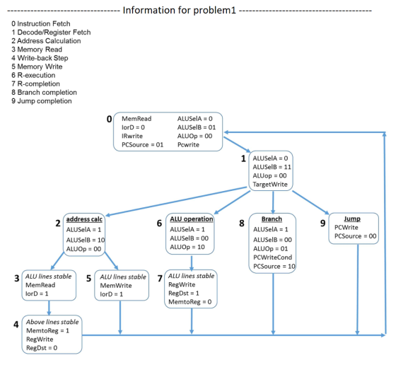
How would the multicycle MIPS design support the jr instruction? Show the machine code format and your solution should describe any new datapath features and control changes to the finite-state diagram below (this may include adding new states).
Homework Answers

Add Answer to:
How would the multicycle MIPS design support the jr instruction?
Show the machine code format and...
*For a clearer view of the datapath* Answer choices for all Consider the MIPS single cycle...
 *For a clearer view of the datapath*
Answer choices for all
Consider the MIPS single cycle datapath shown below. Select the correct control signals that will be generated by the control unit for the following instruction: andi $t0,$t1,4 Instruction (25-01 Shin Jump address (31-0) - left 2) 28 PC +4 [31-28) XCS result left 2 RegDst Jump Branch MemRead Instruction (31-26] MemtoReg Control ALUOP MemWrite ALUSrc RegWrite Instruction (25-21] PC Read address Read register 1 Read Instruction (20-16] Read data...
*For a clearer view of the datapath*
Answer choices for all
Consider the MIPS single cycle datapath shown below. Select the correct control signals that will be generated by the control unit for the following instruction: andi $t0,$t1,4 Instruction (25-01 Shin Jump address (31-0) - left 2) 28 PC +4 [31-28) XCS result left 2 RegDst Jump Branch MemRead Instruction (31-26] MemtoReg Control ALUOP MemWrite ALUSrc RegWrite Instruction (25-21] PC Read address Read register 1 Read Instruction (20-16] Read data...
Q4: Answer the following questions. [7 Marks] The single cycle implementation of MIPS is as shown...
 Q4: Answer the following questions. [7 Marks] The single cycle implementation of MIPS is as shown below. Answer the following questions with reference to "beq $S1, $S2, 8H” instruction. Assume that the contents of the registers S1 = 10 H, S2 = 10H, and PC = 16H, pointing to the instruction under consideration. 1. What is the addressing mode of the instruction? [1] ii. Which part of the instruction format, address of S1 and S2 are stored? [1] 111. What...
it is the same question A block diagram of MIPS architecture is given below. What is...
 it is the same question
A block diagram of MIPS architecture is given below. What is the value of the control bit for each MUX during the execution of the given instruction? Note, you may use N/Aif MUX output is not usefu Add MUX 4 ALU Add, result Shift left 2 RegDst Branch MemRead Instruction (31-26] Control Memto Reg ALUOP Mem Write ALUSrc RegWrite Instruction [25-21) PC Read address Instruction (20-16] MUXT Read register 1 Read Read data 1 register...
it is the same question
A block diagram of MIPS architecture is given below. What is the value of the control bit for each MUX during the execution of the given instruction? Note, you may use N/Aif MUX output is not usefu Add MUX 4 ALU Add, result Shift left 2 RegDst Branch MemRead Instruction (31-26] Control Memto Reg ALUOP Mem Write ALUSrc RegWrite Instruction [25-21) PC Read address Instruction (20-16] MUXT Read register 1 Read Read data 1 register...
The answer to the table given by teacher is: RegDst-0 Jump-x Branch-1 MemRead-1 MemtoReg-x ALUop-1 MemWrite-x...
 The answer to the table given by teacher is:
RegDst-0
Jump-x
Branch-1
MemRead-1
MemtoReg-x
ALUop-1
MemWrite-x
ALUSrc-1 (not sure about this one, please give your answer)
RegWrite-x
x means the signal cannot be set in this instruction.
Could you explain the answer in details?
5. (35 points) We wish to add the single cycle datapath and control. Add an a new instruction im Gump memory) to page. This necessary datapaths and control signals to the attached figure on next new...
The answer to the table given by teacher is:
RegDst-0
Jump-x
Branch-1
MemRead-1
MemtoReg-x
ALUop-1
MemWrite-x
ALUSrc-1 (not sure about this one, please give your answer)
RegWrite-x
x means the signal cannot be set in this instruction.
Could you explain the answer in details?
5. (35 points) We wish to add the single cycle datapath and control. Add an a new instruction im Gump memory) to page. This necessary datapaths and control signals to the attached figure on next new...
Assume that ‘slt $1, $2, $3’ is executed with the implementation in the picture. Identify the value of the 9-bit control...
 Assume that ‘slt $1, $2, $3’ is executed with the implementation
in the picture. Identify the value of the 9-bit control
signals.
Add u X ALU result 4 Add Shift left 2 RegDst Branch MemRead MemtoReg Control ALUOP Instruction [31-26 MemWrite ALUSRC RegWrite Instruction [25-21] Read register 1 Read Read PC address Instruction [20-16] data 1 Read Zero register 2 Instruction ALU ALU 31-0] Instruction memory Read data M Read Address Write result u M Instruction [15-11] register data 2...
Assume that ‘slt $1, $2, $3’ is executed with the implementation
in the picture. Identify the value of the 9-bit control
signals.
Add u X ALU result 4 Add Shift left 2 RegDst Branch MemRead MemtoReg Control ALUOP Instruction [31-26 MemWrite ALUSRC RegWrite Instruction [25-21] Read register 1 Read Read PC address Instruction [20-16] data 1 Read Zero register 2 Instruction ALU ALU 31-0] Instruction memory Read data M Read Address Write result u M Instruction [15-11] register data 2...
(o x Add Addresult ALU Shift left 2 Regst Branch MemRead Instruction (31-26) MemtoReg Controll ALUOP...
 (o x Add Addresult ALU Shift left 2 Regst Branch MemRead Instruction (31-26) MemtoReg Controll ALUOP MemWrite ALUSC RogWrite Instruction [25-21] Read register 1 Read Instruction (20-16) Read data 1 register 2 Write Read Instruction (15-11) Write data Registers PC Read address Zoro ALU ALU Instruction (31-0) Instruction memory result Address Read data register data 2 **039 -25 Write Data data memory Instruction (15-01 16 Sign- extend ALU control Instruction 15-01 With regards to the single cycle implementation (as shown...
A block diagram of MIPS architecture is given below. What is the value of the control...
 A block diagram of MIPS architecture is given below. What is the
value of the control bit for each MUX during the execution of the
given instruction? Note, you may use N/A if MUX output is not
useful.
Add MUX 4 ALU Addresult Shift left 2 RegDst Branch MemRead Instruction (31-26] MemtoReg Control ALUOp MemWrite ALUSrc RegWrite Instruction [25-21] PC Read address Read register 1 Read Read data 1 register 2 Write Read MUX 2 Zero Instruction (2016) MUX(1 Instruction...
A block diagram of MIPS architecture is given below. What is the
value of the control bit for each MUX during the execution of the
given instruction? Note, you may use N/A if MUX output is not
useful.
Add MUX 4 ALU Addresult Shift left 2 RegDst Branch MemRead Instruction (31-26] MemtoReg Control ALUOp MemWrite ALUSrc RegWrite Instruction [25-21] PC Read address Read register 1 Read Read data 1 register 2 Write Read MUX 2 Zero Instruction (2016) MUX(1 Instruction...
3. Assume the processor data path show below. XE30 Add Add ALU result Shift left 2...
 3. Assume the processor data path show below. XE30 Add Add ALU result Shift left 2 RegDst Branch MemRead Instruction (31-26] RegSrc Control ALUOP Mem Write ALUSrc RegWrite PC Instruction (25-21) Read address Instruction (20-16] Instruction [31-0) Instruction instruction (15-11) memory Read register 1 Read data 1 Read register 2 Write Read register data 2 Write data Registers Zero ALU ALU result Read Address data OX OX3) 3x) Write Data data memory Instruction [15-0) 16 32 Sign- extend ALU control...
6. Consider a datapath similar to the one in figure below, but for a processor that only has one type of instruction: unconditional PC-relative branch. What would the cycle time be for this dat...
 6. Consider a datapath similar to the one in figure below, but for a processor that only has one type of instruction: unconditional PC-relative branch. What would the cycle time be for this datapath? PCSrc Add ALU Add result Shift +( left 2 Read register 1 ALUSrc, 4 ALU operation PCRead PC-address Read data 1 Registers Read data 2 MemWrite Zero ALU ALU-I Address MemtoReg Instruction register 2 Instruction | Write Read data-M register Write Lu memory Write Data data...
MCS) Add Addresult ALU Shift left 2 RegDst Branch MemRead MemtoReg Instruction (31-26] Control ALUOP MemWrite...
 MCS) Add Addresult ALU Shift left 2 RegDst Branch MemRead MemtoReg Instruction (31-26] Control ALUOP MemWrite ALUS RegWrite PC instruction (25-21] Instruction (20-16) Read address Instruction (31-0) Instruction memory Read register 1 Read Read data 1 register 2 Write Read Zoro ALU ALU result Address Read data instruction (15-11] register data 2 x3) Write data Registers Write Data data memory Instruction 15-01 16 Sign- extend ALU control Instruction (5-0) With regards to the single cycle implementation (as shown in the...
 *For a clearer view of the datapath*
Answer choices for all
Consider the MIPS single cycle datapath shown below. Select the correct control signals that will be generated by the control unit for the following instruction: andi $t0,$t1,4 Instruction (25-01 Shin Jump address (31-0) - left 2) 28 PC +4 [31-28) XCS result left 2 RegDst Jump Branch MemRead Instruction (31-26] MemtoReg Control ALUOP MemWrite ALUSrc RegWrite Instruction (25-21] PC Read address Read register 1 Read Instruction (20-16] Read data...
*For a clearer view of the datapath*
Answer choices for all
Consider the MIPS single cycle datapath shown below. Select the correct control signals that will be generated by the control unit for the following instruction: andi $t0,$t1,4 Instruction (25-01 Shin Jump address (31-0) - left 2) 28 PC +4 [31-28) XCS result left 2 RegDst Jump Branch MemRead Instruction (31-26] MemtoReg Control ALUOP MemWrite ALUSrc RegWrite Instruction (25-21] PC Read address Read register 1 Read Instruction (20-16] Read data...
 Q4: Answer the following questions. [7 Marks] The single cycle implementation of MIPS is as shown below. Answer the following questions with reference to "beq $S1, $S2, 8H” instruction. Assume that the contents of the registers S1 = 10 H, S2 = 10H, and PC = 16H, pointing to the instruction under consideration. 1. What is the addressing mode of the instruction? [1] ii. Which part of the instruction format, address of S1 and S2 are stored? [1] 111. What...
 it is the same question
A block diagram of MIPS architecture is given below. What is the value of the control bit for each MUX during the execution of the given instruction? Note, you may use N/Aif MUX output is not usefu Add MUX 4 ALU Add, result Shift left 2 RegDst Branch MemRead Instruction (31-26] Control Memto Reg ALUOP Mem Write ALUSrc RegWrite Instruction [25-21) PC Read address Instruction (20-16] MUXT Read register 1 Read Read data 1 register...
it is the same question
A block diagram of MIPS architecture is given below. What is the value of the control bit for each MUX during the execution of the given instruction? Note, you may use N/Aif MUX output is not usefu Add MUX 4 ALU Add, result Shift left 2 RegDst Branch MemRead Instruction (31-26] Control Memto Reg ALUOP Mem Write ALUSrc RegWrite Instruction [25-21) PC Read address Instruction (20-16] MUXT Read register 1 Read Read data 1 register...
 The answer to the table given by teacher is:
RegDst-0
Jump-x
Branch-1
MemRead-1
MemtoReg-x
ALUop-1
MemWrite-x
ALUSrc-1 (not sure about this one, please give your answer)
RegWrite-x
x means the signal cannot be set in this instruction.
Could you explain the answer in details?
5. (35 points) We wish to add the single cycle datapath and control. Add an a new instruction im Gump memory) to page. This necessary datapaths and control signals to the attached figure on next new...
The answer to the table given by teacher is:
RegDst-0
Jump-x
Branch-1
MemRead-1
MemtoReg-x
ALUop-1
MemWrite-x
ALUSrc-1 (not sure about this one, please give your answer)
RegWrite-x
x means the signal cannot be set in this instruction.
Could you explain the answer in details?
5. (35 points) We wish to add the single cycle datapath and control. Add an a new instruction im Gump memory) to page. This necessary datapaths and control signals to the attached figure on next new...
 Assume that ‘slt $1, $2, $3’ is executed with the implementation
in the picture. Identify the value of the 9-bit control
signals.
Add u X ALU result 4 Add Shift left 2 RegDst Branch MemRead MemtoReg Control ALUOP Instruction [31-26 MemWrite ALUSRC RegWrite Instruction [25-21] Read register 1 Read Read PC address Instruction [20-16] data 1 Read Zero register 2 Instruction ALU ALU 31-0] Instruction memory Read data M Read Address Write result u M Instruction [15-11] register data 2...
Assume that ‘slt $1, $2, $3’ is executed with the implementation
in the picture. Identify the value of the 9-bit control
signals.
Add u X ALU result 4 Add Shift left 2 RegDst Branch MemRead MemtoReg Control ALUOP Instruction [31-26 MemWrite ALUSRC RegWrite Instruction [25-21] Read register 1 Read Read PC address Instruction [20-16] data 1 Read Zero register 2 Instruction ALU ALU 31-0] Instruction memory Read data M Read Address Write result u M Instruction [15-11] register data 2...
 (o x Add Addresult ALU Shift left 2 Regst Branch MemRead Instruction (31-26) MemtoReg Controll ALUOP MemWrite ALUSC RogWrite Instruction [25-21] Read register 1 Read Instruction (20-16) Read data 1 register 2 Write Read Instruction (15-11) Write data Registers PC Read address Zoro ALU ALU Instruction (31-0) Instruction memory result Address Read data register data 2 **039 -25 Write Data data memory Instruction (15-01 16 Sign- extend ALU control Instruction 15-01 With regards to the single cycle implementation (as shown...
 A block diagram of MIPS architecture is given below. What is the
value of the control bit for each MUX during the execution of the
given instruction? Note, you may use N/A if MUX output is not
useful.
Add MUX 4 ALU Addresult Shift left 2 RegDst Branch MemRead Instruction (31-26] MemtoReg Control ALUOp MemWrite ALUSrc RegWrite Instruction [25-21] PC Read address Read register 1 Read Read data 1 register 2 Write Read MUX 2 Zero Instruction (2016) MUX(1 Instruction...
A block diagram of MIPS architecture is given below. What is the
value of the control bit for each MUX during the execution of the
given instruction? Note, you may use N/A if MUX output is not
useful.
Add MUX 4 ALU Addresult Shift left 2 RegDst Branch MemRead Instruction (31-26] MemtoReg Control ALUOp MemWrite ALUSrc RegWrite Instruction [25-21] PC Read address Read register 1 Read Read data 1 register 2 Write Read MUX 2 Zero Instruction (2016) MUX(1 Instruction...
 3. Assume the processor data path show below. XE30 Add Add ALU result Shift left 2 RegDst Branch MemRead Instruction (31-26] RegSrc Control ALUOP Mem Write ALUSrc RegWrite PC Instruction (25-21) Read address Instruction (20-16] Instruction [31-0) Instruction instruction (15-11) memory Read register 1 Read data 1 Read register 2 Write Read register data 2 Write data Registers Zero ALU ALU result Read Address data OX OX3) 3x) Write Data data memory Instruction [15-0) 16 32 Sign- extend ALU control...
 6. Consider a datapath similar to the one in figure below, but for a processor that only has one type of instruction: unconditional PC-relative branch. What would the cycle time be for this datapath? PCSrc Add ALU Add result Shift +( left 2 Read register 1 ALUSrc, 4 ALU operation PCRead PC-address Read data 1 Registers Read data 2 MemWrite Zero ALU ALU-I Address MemtoReg Instruction register 2 Instruction | Write Read data-M register Write Lu memory Write Data data...
 MCS) Add Addresult ALU Shift left 2 RegDst Branch MemRead MemtoReg Instruction (31-26] Control ALUOP MemWrite ALUS RegWrite PC instruction (25-21] Instruction (20-16) Read address Instruction (31-0) Instruction memory Read register 1 Read Read data 1 register 2 Write Read Zoro ALU ALU result Address Read data instruction (15-11] register data 2 x3) Write data Registers Write Data data memory Instruction 15-01 16 Sign- extend ALU control Instruction (5-0) With regards to the single cycle implementation (as shown in the...
Most questions answered within 3 hours.
-
Problem #1
The area between Z = 0 and Z = 2.50
The area between Z...
asked 1 hour ago -
1. What is the meaning of the term communication style?
2. What are the benefits to...
asked 58 minutes ago -
9.) You are buying a car that cost $26,500. You make payments of
$412 each month...
asked 1 hour ago -
. Suppose a discrete random variable has probability
distribution
P(x) = .2 if x = 0...
asked 2 hours ago -
Under the influence of its drive force, a snowmobile is moving
at a constant velocity along...
asked 3 hours ago -
Why do organizations decline? What steps can top
management take to halt, decline, and restore organizational...
asked 2 hours ago -
What mechanisms Drive speciation??
(I.e. what was Dawins theory on the orgin of species, and how...
asked 4 hours ago -
The manager at a car assembly plant believes that the mean
assembly time for a car...
asked 5 hours ago -
Which of the following is true of electron capture?
A) It decreases the nuclide's mass number...
asked 6 hours ago -
Assuming an efficiency of 43.10%, calculate the actual yield of
magnesium nitrate formed from 114.9 g...
asked 7 hours ago -
The highly pathogenic bacterium Clostridium
perfringens causes gangrene, a disease that results in the
destruction of...
asked 9 hours ago -
In the context of situation analysis, which of the following is
a category for analysis in...
asked 9 hours ago