
kindly solve and explain the steps and why u took them aswell
Homework Answers

Add Answer to:
kindly solve and explain the steps and why u took them
aswell
Q1. The NMOS and...
EXERCISE 287 5.15 The NMOS and PMOS transistors in the circuit of Fig. E5.15 are matched...
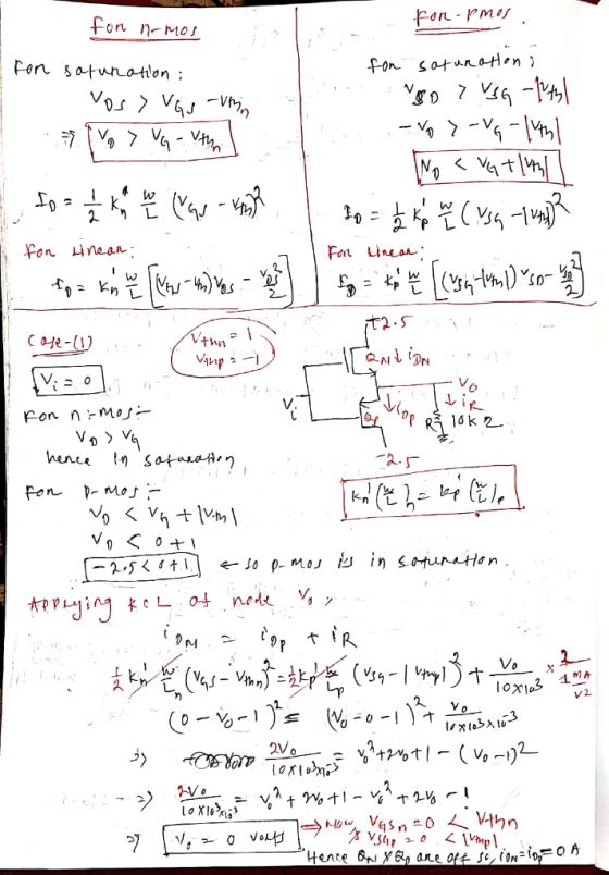
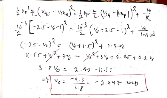
 EXERCISE 287 5.15 The NMOS and PMOS transistors in the circuit of Fig. E5.15 are matched with kn(w,/L, E(WA,) = 1 mA/V2 and V, =-Vp-1 V. Assuming λ=0 for both devices, find the drain currents İDw and įDP and the voltage vo for v,-0 V, +2.5 V, and-2.5 V Ans. o V: 0 mA, O mA. 0V: v- +2.5 V: 0.104 mA, 0mA, 1.04 V: v-2.5 V: 0 mA 0.104 mA, -1.04 V +2.5V ON DN V1 DP -2.5 V...
5. The NMOS and PMOS transistors in the below circuit are matched with kn’(Wn/Ln)=kp'(Wp/Lp)=1 mA/V2 and...
 5. The NMOS and PMOS transistors in the below circuit are matched with kn’(Wn/Ln)=kp'(Wp/Lp)=1 mA/V2 and Vin=-Vt=1V. (20 pts) +5 V a) Which MOSFET is cut-off, NMOS (QN) or PMOS (QP) for VF-5V? Why (5 pts) Qp -5 Vo Ipp Vo VION ON -5 V b) When VF-5V, in which mode, saturation or triode, the circuit operate? Explain why? (5 pts) c) Find the drain current ipy and ipp and the voltage vo for VF-5V (10 pts)
1. Consider the following current mirror combination, where all transistors have the same kn'(W/L...
 1. Consider the following current mirror combination, where all transistors have the same kn'(W/L) = kp'(W/L) = 2mA/V2, and VTN-1У, VTP--1V. It is also given that VDD1-10V, VDD2-8V. Remember that for saturation the drain current is given by IDー½ k,"(W/L) (VGS-Yn)" for NMOS and ID ½ kp"(WL) (VGS-V,»)2 for PMOS. You can ignore the channel modulation for all transistors. (a) Find the value of R so that I.-1mA. (b) Are transistors Q1, Q2, Q3 in saturation? (c) What is the...
All nMOS transistors in the circuit shown are identical, have k' WIL 4 mA/V2 and operate...
 All nMOS transistors in the circuit shown are identical, have k' WIL 4 mA/V2 and operate in the active region lp 1/2k 'W/L(Vas-V)']. Knowing that the de voltage VD4 at the drain of Q4-2 V. Determine: 1. The value of the bias current lo 2. The value of Vov 3. The transconductance gm of Q1 and Q2 4. The voltage gain vo/v 5. The voltage gain when a source resistance R, 1K2 is added to the source of Qi and...
Consider the following current mirror combination, where all transistors have the same kn'(W/L) =...
 Consider the following current mirror
combination, where all transistors have the same
kn'(W/L) =
kp'(W/L) =
2mA/V2, and VTN =
1V, VTP = -1V. It is also given that VDD1 =
10V, VDD2 = 8V. Remember that for saturation the drain
current is given by ID = ½
kn'(W/L)
(VGS –
VTN)2 for NMOS and
ID = ½
kp'(W/L)
(VGS –
VTP)2 for PMOS. You can
ignore the channel modulation for all transistors.
Find the value of R so that...
Consider the following current mirror
combination, where all transistors have the same
kn'(W/L) =
kp'(W/L) =
2mA/V2, and VTN =
1V, VTP = -1V. It is also given that VDD1 =
10V, VDD2 = 8V. Remember that for saturation the drain
current is given by ID = ½
kn'(W/L)
(VGS –
VTN)2 for NMOS and
ID = ½
kp'(W/L)
(VGS –
VTP)2 for PMOS. You can
ignore the channel modulation for all transistors.
Find the value of R so that...
Compute the following for the pseudo-NMOS inverter shown in Figure. VTn=0.45V. VTp=. 0.45V kn-115uA/V2.kp'--304A/V2, VDSATn=0.4V, VDSATp=...
 Compute the following for the pseudo-NMOS inverter shown in Figure. VTn=0.45V. VTp=. 0.45V kn-115uA/V2.kp'--304A/V2, VDSATn=0.4V, VDSATp= -0.4V. Transistors are short channel devices. a. VOL and VOH b. Which is expected to have a higher value? NML or NMH? Why? c. Why is the circuit called a pseudo-NMOS inverter? d. The power dissipation: (1) for Vin low, and (2) for Vin high. Output load is 1 pF e. For an output load of 1 pF, calculate tpLH and tpHL. Are the...
Q1,Q2 and Q3 plz help Question Consider the following inverter design problem: Given VpD 5V, k' 30uA/V , an...
 Q1,Q2 and Q3
plz help
Question Consider the following inverter design problem: Given VpD 5V, k' 30uA/V , and Vo 1V, design a resistive-load inverter circuit with VoL 0.2V . Specifically, determine the (W/L) ratio of the driver transistor and the value of the load resistor RL that achieve the required VoL- (10 marks) Question 2 Consider a pseudo-nMOS NOR2 gate, with the following parameters: 1V., Vro,load -31V, y = 0.4V1/2, andl F|= 0.6V. The transistor Hn Cox =254A/V2, Vro,driver...
Q1,Q2 and Q3
plz help
Question Consider the following inverter design problem: Given VpD 5V, k' 30uA/V , and Vo 1V, design a resistive-load inverter circuit with VoL 0.2V . Specifically, determine the (W/L) ratio of the driver transistor and the value of the load resistor RL that achieve the required VoL- (10 marks) Question 2 Consider a pseudo-nMOS NOR2 gate, with the following parameters: 1V., Vro,load -31V, y = 0.4V1/2, andl F|= 0.6V. The transistor Hn Cox =254A/V2, Vro,driver...
V.+w Operation in the triode reglon Condition v. e Wov 20 Vos uov os os-V (2) p V, so onl+Pala Characteristics Same rel...
 V.+w Operation in the triode reglon Condition v. e Wov 20 Vos uov os os-V (2) p V, so onl+Pala Characteristics Same relationships as for NMOS trasistos tCharacteristics: a CuGs- V,) ®os- } ip.C Replace .and NA with p,,and Nprespectively. V.V V, and yare negative. 2 wov ps For vos 2( -V) e Conditions for operation in the triode region ip lvi Q1. (10 points) For the following configuration of the given figure below, with the following parameters: VDD= +10...
 EXERCISE 287 5.15 The NMOS and PMOS transistors in the circuit of Fig. E5.15 are matched with kn(w,/L, E(WA,) = 1 mA/V2 and V, =-Vp-1 V. Assuming λ=0 for both devices, find the drain currents İDw and įDP and the voltage vo for v,-0 V, +2.5 V, and-2.5 V Ans. o V: 0 mA, O mA. 0V: v- +2.5 V: 0.104 mA, 0mA, 1.04 V: v-2.5 V: 0 mA 0.104 mA, -1.04 V +2.5V ON DN V1 DP -2.5 V...
 5. The NMOS and PMOS transistors in the below circuit are matched with kn’(Wn/Ln)=kp'(Wp/Lp)=1 mA/V2 and Vin=-Vt=1V. (20 pts) +5 V a) Which MOSFET is cut-off, NMOS (QN) or PMOS (QP) for VF-5V? Why (5 pts) Qp -5 Vo Ipp Vo VION ON -5 V b) When VF-5V, in which mode, saturation or triode, the circuit operate? Explain why? (5 pts) c) Find the drain current ipy and ipp and the voltage vo for VF-5V (10 pts)
 1. Consider the following current mirror combination, where all transistors have the same kn'(W/L) = kp'(W/L) = 2mA/V2, and VTN-1У, VTP--1V. It is also given that VDD1-10V, VDD2-8V. Remember that for saturation the drain current is given by IDー½ k,"(W/L) (VGS-Yn)" for NMOS and ID ½ kp"(WL) (VGS-V,»)2 for PMOS. You can ignore the channel modulation for all transistors. (a) Find the value of R so that I.-1mA. (b) Are transistors Q1, Q2, Q3 in saturation? (c) What is the...
 All nMOS transistors in the circuit shown are identical, have k' WIL 4 mA/V2 and operate in the active region lp 1/2k 'W/L(Vas-V)']. Knowing that the de voltage VD4 at the drain of Q4-2 V. Determine: 1. The value of the bias current lo 2. The value of Vov 3. The transconductance gm of Q1 and Q2 4. The voltage gain vo/v 5. The voltage gain when a source resistance R, 1K2 is added to the source of Qi and...
 Consider the following current mirror
combination, where all transistors have the same
kn'(W/L) =
kp'(W/L) =
2mA/V2, and VTN =
1V, VTP = -1V. It is also given that VDD1 =
10V, VDD2 = 8V. Remember that for saturation the drain
current is given by ID = ½
kn'(W/L)
(VGS –
VTN)2 for NMOS and
ID = ½
kp'(W/L)
(VGS –
VTP)2 for PMOS. You can
ignore the channel modulation for all transistors.
Find the value of R so that...
Consider the following current mirror
combination, where all transistors have the same
kn'(W/L) =
kp'(W/L) =
2mA/V2, and VTN =
1V, VTP = -1V. It is also given that VDD1 =
10V, VDD2 = 8V. Remember that for saturation the drain
current is given by ID = ½
kn'(W/L)
(VGS –
VTN)2 for NMOS and
ID = ½
kp'(W/L)
(VGS –
VTP)2 for PMOS. You can
ignore the channel modulation for all transistors.
Find the value of R so that...
 Compute the following for the pseudo-NMOS inverter shown in Figure. VTn=0.45V. VTp=. 0.45V kn-115uA/V2.kp'--304A/V2, VDSATn=0.4V, VDSATp= -0.4V. Transistors are short channel devices. a. VOL and VOH b. Which is expected to have a higher value? NML or NMH? Why? c. Why is the circuit called a pseudo-NMOS inverter? d. The power dissipation: (1) for Vin low, and (2) for Vin high. Output load is 1 pF e. For an output load of 1 pF, calculate tpLH and tpHL. Are the...
 Q1,Q2 and Q3
plz help
Question Consider the following inverter design problem: Given VpD 5V, k' 30uA/V , and Vo 1V, design a resistive-load inverter circuit with VoL 0.2V . Specifically, determine the (W/L) ratio of the driver transistor and the value of the load resistor RL that achieve the required VoL- (10 marks) Question 2 Consider a pseudo-nMOS NOR2 gate, with the following parameters: 1V., Vro,load -31V, y = 0.4V1/2, andl F|= 0.6V. The transistor Hn Cox =254A/V2, Vro,driver...
Q1,Q2 and Q3
plz help
Question Consider the following inverter design problem: Given VpD 5V, k' 30uA/V , and Vo 1V, design a resistive-load inverter circuit with VoL 0.2V . Specifically, determine the (W/L) ratio of the driver transistor and the value of the load resistor RL that achieve the required VoL- (10 marks) Question 2 Consider a pseudo-nMOS NOR2 gate, with the following parameters: 1V., Vro,load -31V, y = 0.4V1/2, andl F|= 0.6V. The transistor Hn Cox =254A/V2, Vro,driver...
 V.+w Operation in the triode reglon Condition v. e Wov 20 Vos uov os os-V (2) p V, so onl+Pala Characteristics Same relationships as for NMOS trasistos tCharacteristics: a CuGs- V,) ®os- } ip.C Replace .and NA with p,,and Nprespectively. V.V V, and yare negative. 2 wov ps For vos 2( -V) e Conditions for operation in the triode region ip lvi Q1. (10 points) For the following configuration of the given figure below, with the following parameters: VDD= +10...
Most questions answered within 3 hours.
-
The
half-life of a radioactive source is 14.0 minutes. How much time
must elapse before the...
asked 2 minutes from now -
A bicyclist starting at rest produces a constant angular
acceleration of 1.10 rad/s2 for wheels that...
asked 4 seconds from now -
Given P(Ec ) = 0.43, P(F) = 0.52, and P(EF) = 0.18.
Find P( E |...
asked 44 minutes ago -
Consider two empty containers A and B whose volumes are
10mL and 20mL respectively. 1mL of...
asked 47 minutes ago -
QUESTION 6
Determine the linear momentum of a 2,800 kg houseboat going 3
m/s.
9,100 kg.m/s...
asked 1 hour ago -
Jor-el throws a ball upward from the top of a 728 foot building
on the planet...
asked 1 hour ago -
Which of the following will most likely to happen if Federal
Reserve Bank decreases the money...
asked 48 minutes ago -
You’ve just joined the investment banking firm of Dewey,
Cheatum, and Howe. They’ve offered you two...
asked 42 minutes ago -
An air conditioner cools 226 m^3/min of humid air at 36 oC and
98% relative humidity...
asked 41 minutes ago -
Vaughn Manufacturing acquires a coal mine at a cost of $1870000.
Intangible development costs total $354000....
asked 51 minutes ago -
Question 5
What effect would a decrease in
temperature have on pressure, assuming that volume
(T)...
asked 1 hour ago -
Draw the Lewis dot structures for the following molecules. None
of the atoms have a formal...
asked 1 hour ago