Consider the following current mirror combination, where all transistors have the same kn'(W/L) =...
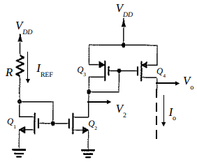
Consider the following current mirror combination, where all transistors have the same kn'(W/L) = kp'(W/L) =
2mA/V2, and VTN = 1V, VTP = -1V. It is also given that VDD1 = 10V, VDD2 = 8V. Remember that for saturation the drain current is given by ID = ½ kn'(W/L) (VGS – VTN)2 for NMOS and ID = ½ kp'(W/L) (VGS – VTP)2 for PMOS. You can ignore the channel modulation for all transistors.
- Find the value of R so that Io=1mA.
- Are transistors Q1, Q2, Q3 in saturation?
- What is the range of Vo so that Q4 is in saturation?
-
Assume that a resistor 1K is connected to the output node (at Vo) as the load (i.e. one terminal of the resistor is connected to the output node, and the other to the ground). Will the particular current mirror support this load? - (e) Assume that a resistor 1K in series to a constant voltage source Vx are connected to the output node (at Vo) as the load (i.e. one terminal of the resistor is connected to the output node and the other to the voltage course. The other voltage source terminal is connected to the ground). What is the allowable voltage range for Vx?
Homework Answers
Add Answer to:
Consider the following current mirror combination, where all transistors have the same kn'(W/L) =...
1. Consider the following current mirror combination, where all transistors have the same kn'(W/L...
 1. Consider the following current mirror combination, where all transistors have the same kn'(W/L) = kp'(W/L) = 2mA/V2, and VTN-1У, VTP--1V. It is also given that VDD1-10V, VDD2-8V. Remember that for saturation the drain current is given by IDー½ k,"(W/L) (VGS-Yn)" for NMOS and ID ½ kp"(WL) (VGS-V,»)2 for PMOS. You can ignore the channel modulation for all transistors. (a) Find the value of R so that I.-1mA. (b) Are transistors Q1, Q2, Q3 in saturation? (c) What is the...
Draw the circuit of a common source amplifier, which is biased by a MOSFET current mirror,...
 Draw the circuit of a common source amplifier, which is biased by a MOSFET current mirror, and which uses only one capacitor and two resistors (including the RREF of the current mirror). Assume that the input to the amplifier is a zero-DC signal. Then, design the amplifier to achieve a gain Avo--gRo =-4V/V, and an output resistance Ro-Ro-1K. Ignore channel modulation. Assume that all MOSFETS are identical with VIN-1V, and Kn = 2mA/V. Use Vo = 5V and Vs =-5V....
I want to understand CMOS 2 stage OP Amp circuit
 kn=100uA/V2, kp=50uA/V2, |VAN|=100V, |VAP|=100V, VTN=VTP=0.8V, W/L of M1 and M2 = 10/1, other transistor’s W/L=10/2, Vg=1.2VI am studying this for exam. but that is so hard to understand...so can you explain this why also? I hope to know about Vcommon min and Vcommon maxLargest Output Voltage and Smallest Output Voltage., Output max souring current, Output Max Sinking current. About this, what will be when Vi = 1V and Vp = 2V? and hope to know OPamp1 and 2's node (1~5), (1~3) and...
Problem #5 The NMOS transistors in the circuits below have V, = 1V and (12)k,'(W/L) =...
 Problem #5 The NMOS transistors in the circuits below have V, = 1V and (12)k,'(W/L) = 1 mA/V2. For each circuit find the operating mode (cutoff, triode, or saturation) and values for VG, ID, VD, and Vs 수+9. 1. 2K 1. 2K 470K 47GK LK 1K
Q5: Consider the following Multistage amplifier with kn' = 160 uA/V?, kp' = 40 A/V, and...
 Q5: Consider the following Multistage amplifier with kn' = 160 uA/V?, kp' = 40 A/V, and Vtn=0.7 V, Vtp=-0.8 V. All the transistors operate at IREF = 90 A , VoV=0.3 V, VA| = 10V for all devices VDD - VSS - 2.5V (Note ID1 = ID2 = ID3 = ID4 = ID5/2 =4541A) and ID5 = ID = ID8 =ID6= Iref (a) Identify the different stages of the amplifiers (b) Design the circuit i.e. find W/L of all transistors...
4) Consider the MOSFET differential amplifier shown below, with Io-2 mA, and RL- 10 kS2, Rss-100 ...
 4) Consider the MOSFET differential amplifier shown below, with Io-2 mA, and RL- 10 kS2, Rss-100 k2, VDD- +8V and Vss--8V. The NMOS transistors in the circuit are nominally identical, with kn 2 mA/V2, VTn 1.0 V and ro 100 k2. The PMoS transistors in the circuit are nominally identical, with kp 2 mA/V2, [VTpl 1.0 V and ro 100 kΩ M3 M4 0 M1 M2 a) First consider the DC bias point. Assuming that the current mirror requires at...
Compute the following for the pseudo-NMOS inverter shown in Figure. VTn=0.45V. VTp=. 0.45V kn-115uA/V2.kp'--304A/V2, VDSATn=0.4V, VDSATp=...
 Compute the following for the pseudo-NMOS inverter shown in Figure. VTn=0.45V. VTp=. 0.45V kn-115uA/V2.kp'--304A/V2, VDSATn=0.4V, VDSATp= -0.4V. Transistors are short channel devices. a. VOL and VOH b. Which is expected to have a higher value? NML or NMH? Why? c. Why is the circuit called a pseudo-NMOS inverter? d. The power dissipation: (1) for Vin low, and (2) for Vin high. Output load is 1 pF e. For an output load of 1 pF, calculate tpLH and tpHL. Are the...
5) Consider the Cascode amplifier shown below. For the NMOS transistors, kn 0.2 mA/V2, Vr,-0.5 V,...
 5) Consider the Cascode amplifier shown below. For the NMOS transistors, kn 0.2 mA/V2, Vr,-0.5 V, (W/L)-(W/L)2-5. VDD-GV and IBIAs= 1.0 mA. a) Assuming λ-0 for all transistors, find the required DC gate- source voltages of M1 and M2 (VGsı and VGs2, respectively) BIAS VD out b) Again assuming 0 M2 for all transistors, what is the minimum DC value of VouT for which the amplifier works in high-gain regime? (W/L)2 in M1 For parts c)-f), Assume -0.01 for all...
Q2: Consider an NMOS FET having W = 160um, L = 2um, Kn' = 50uA/V2, VIN=...
 Q2: Consider an NMOS FET having W = 160um, L = 2um, Kn' = 50uA/V2, VIN= 2V and 2=0. Find out the regions of operation (cut-off, triode, saturation) and the drain current id for the following conditions: a) VGS = 1 V and Vds = 3V b) VGS = 3V and vps = 0.5V c) VGS = 3V and Vds = 5V
2. In the following current mirror circuit, Vcc -10V, and the three transistors, Q1, Q2, Q3, have...
 2. In the following current mirror circuit, Vcc -10V, and the three transistors, Q1, Q2, Q3, have the same saturation current (i.e.,IssIs), and with V for active mode is 0.7V. Then, the three beta values are given by: β91-100, ßQ2-50, and ßQ3-200. The thermal voltage is ντ-25mV. Assuming that you need an output current of i1mA: ref db (a) Find the collector, base, and emitter current for all three Q1 O2 transistors when ia 1mA. (b) Find the refern ie....
 1. Consider the following current mirror combination, where all transistors have the same kn'(W/L) = kp'(W/L) = 2mA/V2, and VTN-1У, VTP--1V. It is also given that VDD1-10V, VDD2-8V. Remember that for saturation the drain current is given by IDー½ k,"(W/L) (VGS-Yn)" for NMOS and ID ½ kp"(WL) (VGS-V,»)2 for PMOS. You can ignore the channel modulation for all transistors. (a) Find the value of R so that I.-1mA. (b) Are transistors Q1, Q2, Q3 in saturation? (c) What is the...
 Draw the circuit of a common source amplifier, which is biased by a MOSFET current mirror, and which uses only one capacitor and two resistors (including the RREF of the current mirror). Assume that the input to the amplifier is a zero-DC signal. Then, design the amplifier to achieve a gain Avo--gRo =-4V/V, and an output resistance Ro-Ro-1K. Ignore channel modulation. Assume that all MOSFETS are identical with VIN-1V, and Kn = 2mA/V. Use Vo = 5V and Vs =-5V....
 Problem #5 The NMOS transistors in the circuits below have V, = 1V and (12)k,'(W/L) = 1 mA/V2. For each circuit find the operating mode (cutoff, triode, or saturation) and values for VG, ID, VD, and Vs 수+9. 1. 2K 1. 2K 470K 47GK LK 1K
 Q5: Consider the following Multistage amplifier with kn' = 160 uA/V?, kp' = 40 A/V, and Vtn=0.7 V, Vtp=-0.8 V. All the transistors operate at IREF = 90 A , VoV=0.3 V, VA| = 10V for all devices VDD - VSS - 2.5V (Note ID1 = ID2 = ID3 = ID4 = ID5/2 =4541A) and ID5 = ID = ID8 =ID6= Iref (a) Identify the different stages of the amplifiers (b) Design the circuit i.e. find W/L of all transistors...
 4) Consider the MOSFET differential amplifier shown below, with Io-2 mA, and RL- 10 kS2, Rss-100 k2, VDD- +8V and Vss--8V. The NMOS transistors in the circuit are nominally identical, with kn 2 mA/V2, VTn 1.0 V and ro 100 k2. The PMoS transistors in the circuit are nominally identical, with kp 2 mA/V2, [VTpl 1.0 V and ro 100 kΩ M3 M4 0 M1 M2 a) First consider the DC bias point. Assuming that the current mirror requires at...
 Compute the following for the pseudo-NMOS inverter shown in Figure. VTn=0.45V. VTp=. 0.45V kn-115uA/V2.kp'--304A/V2, VDSATn=0.4V, VDSATp= -0.4V. Transistors are short channel devices. a. VOL and VOH b. Which is expected to have a higher value? NML or NMH? Why? c. Why is the circuit called a pseudo-NMOS inverter? d. The power dissipation: (1) for Vin low, and (2) for Vin high. Output load is 1 pF e. For an output load of 1 pF, calculate tpLH and tpHL. Are the...
 5) Consider the Cascode amplifier shown below. For the NMOS transistors, kn 0.2 mA/V2, Vr,-0.5 V, (W/L)-(W/L)2-5. VDD-GV and IBIAs= 1.0 mA. a) Assuming λ-0 for all transistors, find the required DC gate- source voltages of M1 and M2 (VGsı and VGs2, respectively) BIAS VD out b) Again assuming 0 M2 for all transistors, what is the minimum DC value of VouT for which the amplifier works in high-gain regime? (W/L)2 in M1 For parts c)-f), Assume -0.01 for all...
 Q2: Consider an NMOS FET having W = 160um, L = 2um, Kn' = 50uA/V2, VIN= 2V and 2=0. Find out the regions of operation (cut-off, triode, saturation) and the drain current id for the following conditions: a) VGS = 1 V and Vds = 3V b) VGS = 3V and vps = 0.5V c) VGS = 3V and Vds = 5V
 2. In the following current mirror circuit, Vcc -10V, and the three transistors, Q1, Q2, Q3, have the same saturation current (i.e.,IssIs), and with V for active mode is 0.7V. Then, the three beta values are given by: β91-100, ßQ2-50, and ßQ3-200. The thermal voltage is ντ-25mV. Assuming that you need an output current of i1mA: ref db (a) Find the collector, base, and emitter current for all three Q1 O2 transistors when ia 1mA. (b) Find the refern ie....
Most questions answered within 3 hours.
-
MAN3240 Organizational Behavior
In one to two paragraphs
6.) How can understanding emotions make me more...
asked 4 minutes ago -
Identify one individual who, in your opinion, is an excellent
leader. List the qualities that this...
asked 1 minute ago -
For the data set shown below, complete parts (a) through (d)
below. x 3 4 5...
asked 7 minutes ago -
A university administrator working in student housing wants to
determine if the percentage of students residing...
asked 21 minutes ago -
3). Describe human population growth that has occurred in the
past 400 years. Use terms learned...
asked 18 minutes ago -
A
projectile is blue at a target. The distance from the point of
impact to the...
asked 43 minutes ago -
Given a 32 bit processor, with 2 MB of physical RAM split into 512
frames. What...
asked 33 minutes ago -
What were the main rulings in the Supreme Court cases which are
Morgan v. Virginia (1946)...
asked 32 minutes ago -
write a five paragraph essay on how setting,
specifically culture, influences the actions of
the characters...
asked 24 minutes ago -
JAVA
Provide a simple code sample of Merge sort
asked 35 minutes ago -
Discounting cash flows involves:
A. taking the cash discount offered on a trade merchandise
B. estimating...
asked 42 minutes ago -
A solid wood door 1.00 m wide and 2.00 m high is hinged along
one side...
asked 42 minutes ago