
Homework Answers

Add Answer to:
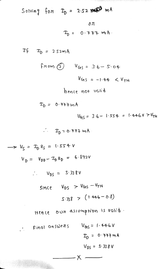
. (lOpts) Calclate Vos lVas in the following figure when VTN -0.8 v K, = 0.5mA/V2,...
2. Calculate VasIVs in the following figure when Vmy 0.8 V, K, 0.5mA/V2 VDD 10V R1...
 2. Calculate VasIVs in the following figure when Vmy 0.8 V, K, 0.5mA/V2 VDD 10V R1 32k RD 4 k 01 NMOS R2 18k RS 2 k
1) For the following four FET circuits, the FET parameters are VTN 2.6Vand KN0.06 A/V2. For...
 1) For the following four FET circuits, the FET parameters are VTN 2.6Vand KN0.06 A/V2. For each circuit, the bias point (Q-point) is the same. A) Find for Vas Vos lo. In all cases, verify that the transistor is "on" and operating ina saturated region. B) On a single, Ip (y-axis) versus Vos (x-axis) plot, sketch the load line for each of the four circuits. Voo+20V Ro" 271 Ω R, 20 ka VoD+10V RG 10 kn RS-729 Ω VDO Voo...
V.+w Operation in the triode reglon Condition v. e Wov 20 Vos uov os os-V (2) p V, so onl+Pala Characteristics Same rel...
 V.+w Operation in the triode reglon Condition v. e Wov 20 Vos uov os os-V (2) p V, so onl+Pala Characteristics Same relationships as for NMOS trasistos tCharacteristics: a CuGs- V,) ®os- } ip.C Replace .and NA with p,,and Nprespectively. V.V V, and yare negative. 2 wov ps For vos 2( -V) e Conditions for operation in the triode region ip lvi Q1. (10 points) For the following configuration of the given figure below, with the following parameters: VDD= +10...
4. Design the circuit of Figure 4 so that the transistor operates in saturation with ID0.5mAand V3V. Let the enhancement-type PMOS transistor have VV and k, (w/L)-1m4/V2. Assume λ-Ο What is the...
 4. Design the circuit of Figure 4 so that the transistor operates in saturation with ID0.5mAand V3V. Let the enhancement-type PMOS transistor have VV and k, (w/L)-1m4/V2. Assume λ-Ο What is the largest value that RD can have while maintaining saturation-region operation? VDD-+5 V o-0.5mA RG2 RG2 RD Figure 4
4. Design the circuit of Figure 4 so that the transistor operates in saturation with ID0.5mAand V3V. Let the enhancement-type PMOS transistor have VV and k, (w/L)-1m4/V2. Assume λ-Ο What...
4. Design the circuit of Figure 4 so that the transistor operates in saturation with ID0.5mAand V3V. Let the enhancement-type PMOS transistor have VV and k, (w/L)-1m4/V2. Assume λ-Ο What is the largest value that RD can have while maintaining saturation-region operation? VDD-+5 V o-0.5mA RG2 RG2 RD Figure 4
4. Design the circuit of Figure 4 so that the transistor operates in saturation with ID0.5mAand V3V. Let the enhancement-type PMOS transistor have VV and k, (w/L)-1m4/V2. Assume λ-Ο What...
1. Compute and plot the curves of ip vs. vps for an FET with Vio-2.5V and K-1 mA/V2 for Vos-2V, 4...
 1. Compute and plot the curves of ip vs. vps for an FET with Vio-2.5V and K-1 mA/V2 for Vos-2V, 4V, 6V, and 8V for 0<VDs<6V. Label the triode region, the saturation region, as well to" GS as the boundary between the two.
1. Compute and plot the curves of ip vs. vps for an FET with Vio-2.5V and K-1 mA/V2 for Vos-2V, 4V, 6V, and 8V for 0
1. Compute and plot the curves of ip vs. vps for an FET with Vio-2.5V and K-1 mA/V2 for Vos-2V, 4V, 6V, and 8V for 0<VDs<6V. Label the triode region, the saturation region, as well to" GS as the boundary between the two.
1. Compute and plot the curves of ip vs. vps for an FET with Vio-2.5V and K-1 mA/V2 for Vos-2V, 4V, 6V, and 8V for 0
Consider an n-channel MOSFET (Von = 0.4 V and K = 3.0 mA/V2). Let VDD =...
 Consider an n-channel MOSFET (Von = 0.4 V and K = 3.0
mA/V2). Let VDD = 5.0 V, VSS =
-5.0 V, R1 = 14.0 kohm, R2 = 6.0 kohm,
RD = 1.2 kohm and RS = 0.5 kohm. Answer the
following questions assuming the transistor is at its saturation
mode.
a) Calculate VG versus ground (not VGS)
(hint: voltage division by R1 and R2 between
VDD and VSS).
b) Calculate VGS. (hint: IDS obtained by
formula = IDS obtained...
Consider an n-channel MOSFET (Von = 0.4 V and K = 3.0
mA/V2). Let VDD = 5.0 V, VSS =
-5.0 V, R1 = 14.0 kohm, R2 = 6.0 kohm,
RD = 1.2 kohm and RS = 0.5 kohm. Answer the
following questions assuming the transistor is at its saturation
mode.
a) Calculate VG versus ground (not VGS)
(hint: voltage division by R1 and R2 between
VDD and VSS).
b) Calculate VGS. (hint: IDS obtained by
formula = IDS obtained...
If you have already answered this please allow someone else solve this... V DD Problem #4:...
 If you have already answered this please allow someone else
solve this...
V DD Problem #4: Design an amplifier based on the circuit to the left. Design for a gain of 10V/V, an input resistance of at least 1M92, and a bias current of 0.1mA. Choose the maximum Rs value that allows the maximum input signal to be amplified and remain linear and in saturation (i.e. use the definition of linear amplification for a FET and saturation). Assume VTN =...
If you have already answered this please allow someone else
solve this...
V DD Problem #4: Design an amplifier based on the circuit to the left. Design for a gain of 10V/V, an input resistance of at least 1M92, and a bias current of 0.1mA. Choose the maximum Rs value that allows the maximum input signal to be amplified and remain linear and in saturation (i.e. use the definition of linear amplification for a FET and saturation). Assume VTN =...
Question 2: a) Find the value of Vgs? b) If the threshold voltage of the NMOS 0.7V, identify the region o...
 Question 2: a) Find the value of Vgs? b) If the threshold voltage of the NMOS 0.7V, identify the region of operation for the MOSFET (i.e. Triode Saturation or Cutoff) v,= 10V SATE e) Write the formula to calculate Current (ID) for the circuit in Figure 1 Fig. 1 Question 3: a) Find the value of Vgs* b) If the threshold voltage of the NMOS 0.7V, identify the region of operation for the MOSFET (i.e. Triode, Saturation or Cutoff) c)...
II) The characteristics of the MOSFET in figure la are shown in figure 1b. Use the characteristic...
 II) The characteristics of the MOSFET in figure la are shown in figure 1b. Use the characteristics in figure 1b, not the equations in your textbook, to answer the following A) From figure lb estimate gm and ro for the FET in the saturation region. Include calculations or an explanation with your answer B Find the values for Re Rd. VDD and VGG so that zin- 100k, zout 5k, L 2 mA and Vds-5 C) Find the GAIN-vo/vi 2oUT Rg...
#4 The accompanying circuit shows a 4-resistor biased JFET transistor Determine the values of Rp and Rs so that the Q-point is equal to, VDsq 10 V and IDg 5 mA . For the JFET take IDss = 10 mA...
 #4
The accompanying circuit shows a 4-resistor biased JFET transistor Determine the values of Rp and Rs so that the Q-point is equal to, VDsq 10 V and IDg 5 mA . For the JFET take IDss = 10 mA, VP =-5 V and λ 0 . The circuit parameters are, R1-740 k, R2-22 1.85 ka, Rs-85 ㏀ and RL-3.5 ㏀. Take the power supply VDD 24 V 2- Vo R1 Vi R2 Signal generator 4-In reference to the circuit...
#4
The accompanying circuit shows a 4-resistor biased JFET transistor Determine the values of Rp and Rs so that the Q-point is equal to, VDsq 10 V and IDg 5 mA . For the JFET take IDss = 10 mA, VP =-5 V and λ 0 . The circuit parameters are, R1-740 k, R2-22 1.85 ka, Rs-85 ㏀ and RL-3.5 ㏀. Take the power supply VDD 24 V 2- Vo R1 Vi R2 Signal generator 4-In reference to the circuit...
 2. Calculate VasIVs in the following figure when Vmy 0.8 V, K, 0.5mA/V2 VDD 10V R1 32k RD 4 k 01 NMOS R2 18k RS 2 k
 1) For the following four FET circuits, the FET parameters are VTN 2.6Vand KN0.06 A/V2. For each circuit, the bias point (Q-point) is the same. A) Find for Vas Vos lo. In all cases, verify that the transistor is "on" and operating ina saturated region. B) On a single, Ip (y-axis) versus Vos (x-axis) plot, sketch the load line for each of the four circuits. Voo+20V Ro" 271 Ω R, 20 ka VoD+10V RG 10 kn RS-729 Ω VDO Voo...
 V.+w Operation in the triode reglon Condition v. e Wov 20 Vos uov os os-V (2) p V, so onl+Pala Characteristics Same relationships as for NMOS trasistos tCharacteristics: a CuGs- V,) ®os- } ip.C Replace .and NA with p,,and Nprespectively. V.V V, and yare negative. 2 wov ps For vos 2( -V) e Conditions for operation in the triode region ip lvi Q1. (10 points) For the following configuration of the given figure below, with the following parameters: VDD= +10...
 4. Design the circuit of Figure 4 so that the transistor operates in saturation with ID0.5mAand V3V. Let the enhancement-type PMOS transistor have VV and k, (w/L)-1m4/V2. Assume λ-Ο What is the largest value that RD can have while maintaining saturation-region operation? VDD-+5 V o-0.5mA RG2 RG2 RD Figure 4
4. Design the circuit of Figure 4 so that the transistor operates in saturation with ID0.5mAand V3V. Let the enhancement-type PMOS transistor have VV and k, (w/L)-1m4/V2. Assume λ-Ο What...
4. Design the circuit of Figure 4 so that the transistor operates in saturation with ID0.5mAand V3V. Let the enhancement-type PMOS transistor have VV and k, (w/L)-1m4/V2. Assume λ-Ο What is the largest value that RD can have while maintaining saturation-region operation? VDD-+5 V o-0.5mA RG2 RG2 RD Figure 4
4. Design the circuit of Figure 4 so that the transistor operates in saturation with ID0.5mAand V3V. Let the enhancement-type PMOS transistor have VV and k, (w/L)-1m4/V2. Assume λ-Ο What...
 1. Compute and plot the curves of ip vs. vps for an FET with Vio-2.5V and K-1 mA/V2 for Vos-2V, 4V, 6V, and 8V for 0<VDs<6V. Label the triode region, the saturation region, as well to" GS as the boundary between the two.
1. Compute and plot the curves of ip vs. vps for an FET with Vio-2.5V and K-1 mA/V2 for Vos-2V, 4V, 6V, and 8V for 0
1. Compute and plot the curves of ip vs. vps for an FET with Vio-2.5V and K-1 mA/V2 for Vos-2V, 4V, 6V, and 8V for 0<VDs<6V. Label the triode region, the saturation region, as well to" GS as the boundary between the two.
1. Compute and plot the curves of ip vs. vps for an FET with Vio-2.5V and K-1 mA/V2 for Vos-2V, 4V, 6V, and 8V for 0
 Consider an n-channel MOSFET (Von = 0.4 V and K = 3.0
mA/V2). Let VDD = 5.0 V, VSS =
-5.0 V, R1 = 14.0 kohm, R2 = 6.0 kohm,
RD = 1.2 kohm and RS = 0.5 kohm. Answer the
following questions assuming the transistor is at its saturation
mode.
a) Calculate VG versus ground (not VGS)
(hint: voltage division by R1 and R2 between
VDD and VSS).
b) Calculate VGS. (hint: IDS obtained by
formula = IDS obtained...
Consider an n-channel MOSFET (Von = 0.4 V and K = 3.0
mA/V2). Let VDD = 5.0 V, VSS =
-5.0 V, R1 = 14.0 kohm, R2 = 6.0 kohm,
RD = 1.2 kohm and RS = 0.5 kohm. Answer the
following questions assuming the transistor is at its saturation
mode.
a) Calculate VG versus ground (not VGS)
(hint: voltage division by R1 and R2 between
VDD and VSS).
b) Calculate VGS. (hint: IDS obtained by
formula = IDS obtained...
 If you have already answered this please allow someone else
solve this...
V DD Problem #4: Design an amplifier based on the circuit to the left. Design for a gain of 10V/V, an input resistance of at least 1M92, and a bias current of 0.1mA. Choose the maximum Rs value that allows the maximum input signal to be amplified and remain linear and in saturation (i.e. use the definition of linear amplification for a FET and saturation). Assume VTN =...
If you have already answered this please allow someone else
solve this...
V DD Problem #4: Design an amplifier based on the circuit to the left. Design for a gain of 10V/V, an input resistance of at least 1M92, and a bias current of 0.1mA. Choose the maximum Rs value that allows the maximum input signal to be amplified and remain linear and in saturation (i.e. use the definition of linear amplification for a FET and saturation). Assume VTN =...
 Question 2: a) Find the value of Vgs? b) If the threshold voltage of the NMOS 0.7V, identify the region of operation for the MOSFET (i.e. Triode Saturation or Cutoff) v,= 10V SATE e) Write the formula to calculate Current (ID) for the circuit in Figure 1 Fig. 1 Question 3: a) Find the value of Vgs* b) If the threshold voltage of the NMOS 0.7V, identify the region of operation for the MOSFET (i.e. Triode, Saturation or Cutoff) c)...
 II) The characteristics of the MOSFET in figure la are shown in figure 1b. Use the characteristics in figure 1b, not the equations in your textbook, to answer the following A) From figure lb estimate gm and ro for the FET in the saturation region. Include calculations or an explanation with your answer B Find the values for Re Rd. VDD and VGG so that zin- 100k, zout 5k, L 2 mA and Vds-5 C) Find the GAIN-vo/vi 2oUT Rg...
 #4
The accompanying circuit shows a 4-resistor biased JFET transistor Determine the values of Rp and Rs so that the Q-point is equal to, VDsq 10 V and IDg 5 mA . For the JFET take IDss = 10 mA, VP =-5 V and λ 0 . The circuit parameters are, R1-740 k, R2-22 1.85 ka, Rs-85 ㏀ and RL-3.5 ㏀. Take the power supply VDD 24 V 2- Vo R1 Vi R2 Signal generator 4-In reference to the circuit...
#4
The accompanying circuit shows a 4-resistor biased JFET transistor Determine the values of Rp and Rs so that the Q-point is equal to, VDsq 10 V and IDg 5 mA . For the JFET take IDss = 10 mA, VP =-5 V and λ 0 . The circuit parameters are, R1-740 k, R2-22 1.85 ka, Rs-85 ㏀ and RL-3.5 ㏀. Take the power supply VDD 24 V 2- Vo R1 Vi R2 Signal generator 4-In reference to the circuit...
Most questions answered within 3 hours.
-
The energy released by each fission within the core of a nuclear
reactor is 2.00 ×...
asked 1 hour ago -
In the ____ effects ANOVA design, the experimenter is interested
in generalizing to other levels ot...
asked 2 hours ago -
Questions 31-32: Consider the following table of data. We want
to know if there is an...
asked 2 hours ago -
How does myoblast and myotube differs in cytoskeletal
components of their microfilaments (actin), microtubules (tubulin),
and...
asked 3 hours ago -
A buffer solution contains 0.322 M ammonium chloride and 0.486 M
ammonia. If 0.0545 moles of...
asked 3 hours ago -
You and a friend play a game where you roll a die. If an even
number...
asked 5 hours ago -
Java Programming
A program is required to calculate the amount of paint needed for
painting a...
asked 6 hours ago -
Meg Prior is 25 years old and is going to invest $10,000 in her
retirement fund...
asked 4 hours ago -
SANDY OWNS A BEACH HOME IN FLORIDA. IF HOME RENTED FOR 300 DAYS
DURING THE YEAR,...
asked 6 hours ago -
What do we mean by security certificate. Please explain with
examples.
Please explain the examples the...
asked 4 hours ago -
4. Complete Table below based on the10 plots of Magnetic Field
vs. Current graph with the...
asked 4 hours ago -
Prepare 100.00ml of 0.10M HCl (stock solution of 3.00M
available)
asked 5 hours ago