
Homework Answers

Add Answer to:
Problem 5 Given the following circuit, assume the following parameters VBB IV, RB 220 k, RC...
5 نقاط For the circuit shown, If there is an added 1 K. Ohm resistor at...
 5 نقاط For the circuit shown, If there is an added 1 K. Ohm resistor at the emitter terminal connected between Emitter and Ground, then calculate IB, IC, VCE, VB, and VC knowing that Vcc = 12 Volts, RB = 220 K. Ohm, RC = 4 K. Ohm, VBE = 0.7 volts, and Beta of transistor = 50 VCC Fig. 1 Rc im Ic RB ac HE output signal C2 IB + ac VCE input I signal G B +...
4.3V (15 pts) For the circuit shown, Rc = 2 kQ. Assume that VBE-0.7V, and that...
 4.3V (15 pts) For the circuit shown, Rc = 2 kQ. Assume that VBE-0.7V, and that β very large, resulting in the emitter and collector currents being about equal. a) Determine the value of RE that would result in VcE 3V b) Determine the value of the collector current. c) Determine the value of β, if the base current IB-2μΑ. RE -5.7V
4. Lab VIII: Experiment VII The Bipolar Junction Transistor (BJT) Characteristics The bipolar junction transistor (BJT)...
 4. Lab VIII: Experiment VII The Bipolar Junction Transistor (BJT) Characteristics The bipolar junction transistor (BJT) is a three-terminal solid state device widely used as an amplifier (or switching) device. It consists of two n-type materials sandwiched by p-type material (npn) or two p-type and n-type. The terminals (sections) are known as emitter E, base B and collector C. Two currents and two voltages uniquely describe the behavior of the device. The third current/voltage can be determined through KCL/KVL. See...
Given RB = 240 k., Rc = 1.2 k., and = 120. Determine: a) IB b)...
 Given RB = 240 k., Rc = 1.2 k., and = 120. Determine: a) IB b) Ic c) le d) VBE e) VCE f) Mode of operation (cutoff, active, saturation) Given RB = 47 kO2, Rc = 1.2 k2 and B = 120. Determine: g) Mode of operation (cutoff, active, saturation) O 8V For the circuit shown in Question #2, Vcc = 16 V, RB = 620 kl, Rc = 2 kN and B = 120. a) Determine le b)...
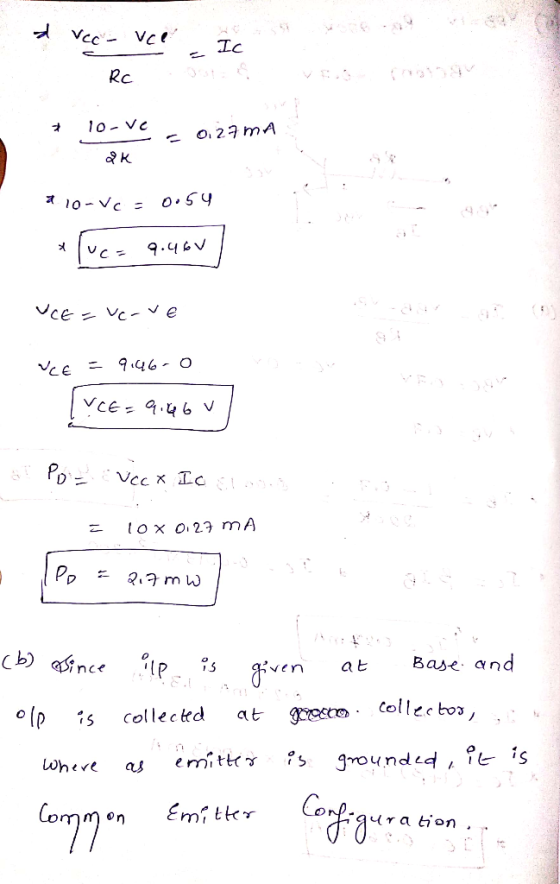
4. VBB= 10 V RB 200 k Vcc 20 V Rc 1k Using the second approximation...
 4. VBB= 10 V RB 200 k Vcc 20 V Rc 1k Using the second approximation of a transistor, solve for Bn 100 Icat) mA VCE(cut) V HA Ic = mA Ig = mA VE= V VB = V Vc = V VCE = V Pp= mW Draw load line Draw Q point Tle 20 15 10 5 Vce 25 20 15 10 5 For Bmax 300 For Bmin 30 mA mA VCE= _V VCE= V Oh Transistors Me se...
1. Consider the emitter-stabilized circuit shown below Vcc-15V RB 430kΩ Rc 1.6k2 IB β = 125...
 1. Consider the emitter-stabilized circuit shown below Vcc-15V RB 430kΩ Rc 1.6k2 IB β = 125 RE a) Find b, k, and VCE for the circuit as shown, with β = 125 b) Suppose that β can vary in the range from 100 to 150 due to manufacturing variations. What is the resulting range in Vce? c) What is the requirement on β such that the transistor will not saturate?
Experiment 2: Good biasing Set up the circuit with R2 12 k2, R RE 1 k, and Vcc 15 V 39 k2, Rc = 2 k?. Circuit An...
 Experiment 2: Good biasing Set up the circuit with R2 12 k2, R RE 1 k, and Vcc 15 V 39 k2, Rc = 2 k?. Circuit Analysis: Compute Ic, I, and VCE PSpice Simulation: a) Simulate the circuit with PSpice (bias point details only) and compare values of Ic, IB, VCE, and VBE from PSpice simulations with your analytical calculations. b) Rerun your PSpice simulations for temperatures of 0 and 60°C. Make a table of Ic IB, VCE, and...
Q.11. Calculate the base, collector and emitter currents for the circuit given in Fig. 01. Also,...
 Q.11. Calculate the base, collector and emitter currents for the circuit given in Fig. 01. Also, determine the value of the voltage drop between collecter and emitter (Ve). Assume that the transistor is in active region and the value current amplification factor is 200. Given that the base-emitter voltage V is 0.7 V. Vcc - 10V 21 Ves = 4V W 220 KS2 Fig. Q11
The 1 mA. V, ls -VE -15 15 V, in the following differential amplifier circuit, Vcc parameters are given as β, 100, VBE# 0.7 V, pr-25 mV, K.-100 V. transistor Rc-10 kΩ For: RE-150 Ω Rc Rc REE-200...
 The 1 mA. V, ls -VE -15 15 V, in the following differential amplifier circuit, Vcc parameters are given as β, 100, VBE# 0.7 V, pr-25 mV, K.-100 V. transistor Rc-10 kΩ For: RE-150 Ω Rc Rc REE-200 kΩ a) What is the input differential resistance, Rid b) What is the overall voltage gain vV? You c) What is input common mode resistance, d) What is the worst case common mode gain that appear across the two input terminals? (4...
1) Consider the following circuit with an assumption that we have the transistor in active mode....
 1) Consider the following circuit with an assumption that we have the transistor in active mode. The type of circuit below is a transistor commonn-emitter circuit. You must firstly determine i) Is then secondly ii) I and finally ii) Vce. All working must be shown. Rc 1.06.12 RB w @ Bpc = 50 + Vcc 10 V + 10 ΚΩ VBB 3 V
 5 نقاط For the circuit shown, If there is an added 1 K. Ohm resistor at the emitter terminal connected between Emitter and Ground, then calculate IB, IC, VCE, VB, and VC knowing that Vcc = 12 Volts, RB = 220 K. Ohm, RC = 4 K. Ohm, VBE = 0.7 volts, and Beta of transistor = 50 VCC Fig. 1 Rc im Ic RB ac HE output signal C2 IB + ac VCE input I signal G B +...
 4.3V (15 pts) For the circuit shown, Rc = 2 kQ. Assume that VBE-0.7V, and that β very large, resulting in the emitter and collector currents being about equal. a) Determine the value of RE that would result in VcE 3V b) Determine the value of the collector current. c) Determine the value of β, if the base current IB-2μΑ. RE -5.7V
 4. Lab VIII: Experiment VII The Bipolar Junction Transistor (BJT) Characteristics The bipolar junction transistor (BJT) is a three-terminal solid state device widely used as an amplifier (or switching) device. It consists of two n-type materials sandwiched by p-type material (npn) or two p-type and n-type. The terminals (sections) are known as emitter E, base B and collector C. Two currents and two voltages uniquely describe the behavior of the device. The third current/voltage can be determined through KCL/KVL. See...
 Given RB = 240 k., Rc = 1.2 k., and = 120. Determine: a) IB b) Ic c) le d) VBE e) VCE f) Mode of operation (cutoff, active, saturation) Given RB = 47 kO2, Rc = 1.2 k2 and B = 120. Determine: g) Mode of operation (cutoff, active, saturation) O 8V For the circuit shown in Question #2, Vcc = 16 V, RB = 620 kl, Rc = 2 kN and B = 120. a) Determine le b)...
 4. VBB= 10 V RB 200 k Vcc 20 V Rc 1k Using the second approximation of a transistor, solve for Bn 100 Icat) mA VCE(cut) V HA Ic = mA Ig = mA VE= V VB = V Vc = V VCE = V Pp= mW Draw load line Draw Q point Tle 20 15 10 5 Vce 25 20 15 10 5 For Bmax 300 For Bmin 30 mA mA VCE= _V VCE= V Oh Transistors Me se...
 1. Consider the emitter-stabilized circuit shown below Vcc-15V RB 430kΩ Rc 1.6k2 IB β = 125 RE a) Find b, k, and VCE for the circuit as shown, with β = 125 b) Suppose that β can vary in the range from 100 to 150 due to manufacturing variations. What is the resulting range in Vce? c) What is the requirement on β such that the transistor will not saturate?
 Experiment 2: Good biasing Set up the circuit with R2 12 k2, R RE 1 k, and Vcc 15 V 39 k2, Rc = 2 k?. Circuit Analysis: Compute Ic, I, and VCE PSpice Simulation: a) Simulate the circuit with PSpice (bias point details only) and compare values of Ic, IB, VCE, and VBE from PSpice simulations with your analytical calculations. b) Rerun your PSpice simulations for temperatures of 0 and 60°C. Make a table of Ic IB, VCE, and...
 Q.11. Calculate the base, collector and emitter currents for the circuit given in Fig. 01. Also, determine the value of the voltage drop between collecter and emitter (Ve). Assume that the transistor is in active region and the value current amplification factor is 200. Given that the base-emitter voltage V is 0.7 V. Vcc - 10V 21 Ves = 4V W 220 KS2 Fig. Q11
 The 1 mA. V, ls -VE -15 15 V, in the following differential amplifier circuit, Vcc parameters are given as β, 100, VBE# 0.7 V, pr-25 mV, K.-100 V. transistor Rc-10 kΩ For: RE-150 Ω Rc Rc REE-200 kΩ a) What is the input differential resistance, Rid b) What is the overall voltage gain vV? You c) What is input common mode resistance, d) What is the worst case common mode gain that appear across the two input terminals? (4...
 1) Consider the following circuit with an assumption that we have the transistor in active mode. The type of circuit below is a transistor commonn-emitter circuit. You must firstly determine i) Is then secondly ii) I and finally ii) Vce. All working must be shown. Rc 1.06.12 RB w @ Bpc = 50 + Vcc 10 V + 10 ΚΩ VBB 3 V
Most questions answered within 3 hours.
-
2. How long would it take for 1.50 mol of water at 100.0 ∘C to
be...
asked 12 minutes ago -
According to the February 2008 Federal Trade Commission report
on consumer fraud and identity theft, 23%...
asked 24 minutes ago -
Data is only as good as its completeness. And we have all dealt
with incomplete data....
asked 19 minutes ago -
Design a Class Diagram for a game of Dots and Boxes
that can do the
following:...
asked 25 minutes ago -
Describe the Christian Anfinsen’s experimentS AND explain how
they have resulted in our current understanding of...
asked 34 minutes ago -
Do a research and write about the below areas of
SPAIN country business activities (GLOBAL
BUSINESS)...
asked 37 minutes ago -
Production and operations management involves three main types
of decisions that are made at three different...
asked 38 minutes ago -
When parked, your car is 6.4 m long. Unfortunately, your garage
is only 3.9 m long....
asked 48 minutes ago -
Use Python 3 in Jupyter
Write a function called countUnique that has one parameter which
is...
asked 46 minutes ago -
The WRT Corporation makes collections on sales according to the
following schedule:
30% in month of...
asked 53 minutes ago -
2C4H18O4+13O2=8CO2+18H2O
how many atoms of oxygen are required to generate 10.3 g of
carbon dioxide?
asked 1 hour ago -
Based on USDA estimates, the cross-price elasticity for peanut
butter consumption with respect to grape jam...
asked 1 hour ago