For the circuit below, NEED HELP ASAP
Homework Answers

Add Answer to:
For the circuit below, NEED HELP ASAP
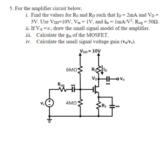
5. For the amplifier circuit below, i. Find the...
Exercise 7.37: Design the bias circuit for the CS amplifier. Assume the MOSFET is specified to...
 Exercise 7.37: Design the bias circuit for the CS amplifier. Assume the MOSFET is specified to have Vt 1 V, kn = 4mA/V2 and V4 = 100 V. Neglecting the Early effect, design for ID-0.5mA, VS= 3.5 V, VD6 V and VDD 15 V. Specify the values of RD and Rs If a current of 2 μΑ is used in the voltage divider, specify the values of RG1 and RG2. Give the values of the MOSFET parameters gm and ro...
Design a common-source MOSFET amplifier such that - Rg is a multiple of 10 - Id...
Design a common-source MOSFET amplifier such that - Rg is a multiple of 10 - Id = 0.52 mA - the amplifier input resistance is in the range of mega ohms - | Avo | = 16.7 V/V - RL = 20k - Vsig has a 2kHz frequency - Rsig = 400k, and is the input and the MOSFET has: Vt = 0.8V k = 5 mA/V^2 VA = 80 V Assume capacitors are shorted in the signal circuit and...
Also please solve for the Gain Determine values for all resistors in the biasing circuit of...
 Also please solve for the
Gain
Determine values for all resistors in the biasing circuit of a Common Source n- MOSFET Amplifier configuration. VDD VDD 9V 9V RG2 Assume kn = 2 mA/V2, Vtn = 1 V and VA = 00. قش NMOS_db_3port* • Q1 is biased in the saturation region • 10 = 1mA SRG2 >RS • Rin ~10 M12
Also please solve for the
Gain
Determine values for all resistors in the biasing circuit of a Common Source n- MOSFET Amplifier configuration. VDD VDD 9V 9V RG2 Assume kn = 2 mA/V2, Vtn = 1 V and VA = 00. قش NMOS_db_3port* • Q1 is biased in the saturation region • 10 = 1mA SRG2 >RS • Rin ~10 M12
Design a common-source MOSFET amplifier such that RG is a multiple of D = o.st mot...
 Design a common-source MOSFET amplifier such that RG is a multiple of D = o.st mot (Avol 15.02 VN RL = 17kr • Choose a sinusoidal signal voltage, Vsig, with Rsig = 400 kN to use as the input in this problem. Use 2 kHz as the frequency of your sinusoidal. This is a design problem so vsig will not be unique. Use V+ = 0.8 V, k = 5 mA/V2, and VA = 80 V for your MOSFET. Assume...
V.+w Operation in the triode reglon Condition v. e Wov 20 Vos uov os os-V (2) p V, so onl+Pala Characteristics Same rel...
 V.+w Operation in the triode reglon Condition v. e Wov 20 Vos uov os os-V (2) p V, so onl+Pala Characteristics Same relationships as for NMOS trasistos tCharacteristics: a CuGs- V,) ®os- } ip.C Replace .and NA with p,,and Nprespectively. V.V V, and yare negative. 2 wov ps For vos 2( -V) e Conditions for operation in the triode region ip lvi Q1. (10 points) For the following configuration of the given figure below, with the following parameters: VDD= +10...
please answer this ASAP Answer the following questions for the below BJT amplifier circuit. Assume capacitors...
 please answer this ASAP
Answer the following questions for the below BJT amplifier circuit. Assume capacitors are short in the signal circuit. Use Vr 25 mV,B = 100, Vpo = 0.7 V, and Ignore the early effect in the bias and signal circuits Find the Bias parameters of the amplifier circuit a) b) Find the small signal parameters of the amplifier. c) Draw the small signal equivalent circuit. Find the open loop voltage gain (Ayo), voltage gain (A,), total circuit...
please answer this ASAP
Answer the following questions for the below BJT amplifier circuit. Assume capacitors are short in the signal circuit. Use Vr 25 mV,B = 100, Vpo = 0.7 V, and Ignore the early effect in the bias and signal circuits Find the Bias parameters of the amplifier circuit a) b) Find the small signal parameters of the amplifier. c) Draw the small signal equivalent circuit. Find the open loop voltage gain (Ayo), voltage gain (A,), total circuit...
Q6. An amplifier circuit using an n-MOSFET is shown in Fig. Q6. The n-MOSFET has the...
 Q6. An amplifier circuit using an n-MOSFET is shown in Fig. Q6. The n-MOSFET has the following parameters: K'-1 mA/V2 and λ-0.02 w. v°' is a small signal AC voltage ource 8V 8V Vout Ra 2.56 mA Fig. Q6 (a) Calculate the DC gate voltage, Va. (b) Assuming that the n-MOSFET is operating in the saturation region and neglecting channel length modulation, calculate the threshold voltage, VrHN, given that the voltage drop across the de current sorce, Inas, has been...
VDD RD RG1 out Vin G2 Figure 3 Design your own common source amplifier based on...
 VDD RD RG1 out Vin G2 Figure 3 Design your own common source amplifier based on Figure 3. You need an input resistance Rin 1M2. Make VD 2Voo/3, Vs Voo/3. Use VG 5 [V]. VoD 10 [V] a. Draw the small signal equivalent circuit b. Find RG1, and RG2, and lo c. Choose values of Ro, and Rs d. Find gm, and Av-Vout/Vin
3. The following figure shows a discrete circuit CS amplifier with a feedback biasing. The nMOS...
 3. The following figure shows a discrete circuit CS amplifier with a feedback biasing. The nMOS has Vt =1V, ?nCoxw/L=0.2mA/V2,and VA-50V ? Calculate ID, VGS and VD. 2 Find gm and ro 3 Find Rn and vo/v.
MOSFET design, KCL, KVL, nmos, pmos 40μΑ Qi. Consider the amplifier shown below. Assume the MOSFET...
 MOSFET design, KCL, KVL, nmos, pmos
40μΑ Qi. Consider the amplifier shown below. Assume the MOSFET has K,-- V. IV, Cg,-0.8pF, Cgdー0.2pF and no body effect. Given RB-100Rs, RREF the small signal AC gain is -1.6. 4kQand (a) Design RB and Rs so that the fu is 40MHz (b) Design CL so that the fi is 50Hz. 10V Mi RREF RB Rs M2 CL RD 1 00kΩ
MOSFET design, KCL, KVL, nmos, pmos
40μΑ Qi. Consider the amplifier shown below. Assume the MOSFET has K,-- V. IV, Cg,-0.8pF, Cgdー0.2pF and no body effect. Given RB-100Rs, RREF the small signal AC gain is -1.6. 4kQand (a) Design RB and Rs so that the fu is 40MHz (b) Design CL so that the fi is 50Hz. 10V Mi RREF RB Rs M2 CL RD 1 00kΩ
 Exercise 7.37: Design the bias circuit for the CS amplifier. Assume the MOSFET is specified to have Vt 1 V, kn = 4mA/V2 and V4 = 100 V. Neglecting the Early effect, design for ID-0.5mA, VS= 3.5 V, VD6 V and VDD 15 V. Specify the values of RD and Rs If a current of 2 μΑ is used in the voltage divider, specify the values of RG1 and RG2. Give the values of the MOSFET parameters gm and ro...
 Also please solve for the
Gain
Determine values for all resistors in the biasing circuit of a Common Source n- MOSFET Amplifier configuration. VDD VDD 9V 9V RG2 Assume kn = 2 mA/V2, Vtn = 1 V and VA = 00. قش NMOS_db_3port* • Q1 is biased in the saturation region • 10 = 1mA SRG2 >RS • Rin ~10 M12
Also please solve for the
Gain
Determine values for all resistors in the biasing circuit of a Common Source n- MOSFET Amplifier configuration. VDD VDD 9V 9V RG2 Assume kn = 2 mA/V2, Vtn = 1 V and VA = 00. قش NMOS_db_3port* • Q1 is biased in the saturation region • 10 = 1mA SRG2 >RS • Rin ~10 M12
 Design a common-source MOSFET amplifier such that RG is a multiple of D = o.st mot (Avol 15.02 VN RL = 17kr • Choose a sinusoidal signal voltage, Vsig, with Rsig = 400 kN to use as the input in this problem. Use 2 kHz as the frequency of your sinusoidal. This is a design problem so vsig will not be unique. Use V+ = 0.8 V, k = 5 mA/V2, and VA = 80 V for your MOSFET. Assume...
 V.+w Operation in the triode reglon Condition v. e Wov 20 Vos uov os os-V (2) p V, so onl+Pala Characteristics Same relationships as for NMOS trasistos tCharacteristics: a CuGs- V,) ®os- } ip.C Replace .and NA with p,,and Nprespectively. V.V V, and yare negative. 2 wov ps For vos 2( -V) e Conditions for operation in the triode region ip lvi Q1. (10 points) For the following configuration of the given figure below, with the following parameters: VDD= +10...
 please answer this ASAP
Answer the following questions for the below BJT amplifier circuit. Assume capacitors are short in the signal circuit. Use Vr 25 mV,B = 100, Vpo = 0.7 V, and Ignore the early effect in the bias and signal circuits Find the Bias parameters of the amplifier circuit a) b) Find the small signal parameters of the amplifier. c) Draw the small signal equivalent circuit. Find the open loop voltage gain (Ayo), voltage gain (A,), total circuit...
please answer this ASAP
Answer the following questions for the below BJT amplifier circuit. Assume capacitors are short in the signal circuit. Use Vr 25 mV,B = 100, Vpo = 0.7 V, and Ignore the early effect in the bias and signal circuits Find the Bias parameters of the amplifier circuit a) b) Find the small signal parameters of the amplifier. c) Draw the small signal equivalent circuit. Find the open loop voltage gain (Ayo), voltage gain (A,), total circuit...
 Q6. An amplifier circuit using an n-MOSFET is shown in Fig. Q6. The n-MOSFET has the following parameters: K'-1 mA/V2 and λ-0.02 w. v°' is a small signal AC voltage ource 8V 8V Vout Ra 2.56 mA Fig. Q6 (a) Calculate the DC gate voltage, Va. (b) Assuming that the n-MOSFET is operating in the saturation region and neglecting channel length modulation, calculate the threshold voltage, VrHN, given that the voltage drop across the de current sorce, Inas, has been...
 VDD RD RG1 out Vin G2 Figure 3 Design your own common source amplifier based on Figure 3. You need an input resistance Rin 1M2. Make VD 2Voo/3, Vs Voo/3. Use VG 5 [V]. VoD 10 [V] a. Draw the small signal equivalent circuit b. Find RG1, and RG2, and lo c. Choose values of Ro, and Rs d. Find gm, and Av-Vout/Vin
 3. The following figure shows a discrete circuit CS amplifier with a feedback biasing. The nMOS has Vt =1V, ?nCoxw/L=0.2mA/V2,and VA-50V ? Calculate ID, VGS and VD. 2 Find gm and ro 3 Find Rn and vo/v.
 MOSFET design, KCL, KVL, nmos, pmos
40μΑ Qi. Consider the amplifier shown below. Assume the MOSFET has K,-- V. IV, Cg,-0.8pF, Cgdー0.2pF and no body effect. Given RB-100Rs, RREF the small signal AC gain is -1.6. 4kQand (a) Design RB and Rs so that the fu is 40MHz (b) Design CL so that the fi is 50Hz. 10V Mi RREF RB Rs M2 CL RD 1 00kΩ
MOSFET design, KCL, KVL, nmos, pmos
40μΑ Qi. Consider the amplifier shown below. Assume the MOSFET has K,-- V. IV, Cg,-0.8pF, Cgdー0.2pF and no body effect. Given RB-100Rs, RREF the small signal AC gain is -1.6. 4kQand (a) Design RB and Rs so that the fu is 40MHz (b) Design CL so that the fi is 50Hz. 10V Mi RREF RB Rs M2 CL RD 1 00kΩ
Most questions answered within 3 hours.
-
just another way of saying good target marketing and
understanding customer needs? Why or why not?
asked 42 minutes ago -
Consider the quantum number sets listed below.
What is the name of the smallest element for...
asked 2 hours ago -
In python,write a function nameSet(first, last) that takes a
person's first and last names as input,...
asked 4 hours ago -
How do you think we should value management? Specifically how
might we try to determine MRPL...
asked 4 hours ago -
Suppose the Central Bank of Turkey starts to pay
interest on reserves. Under what circumstances this...
asked 4 hours ago -
For Bergson the concept of Being contains less reality than does
the concept of Becoming. True...
asked 5 hours ago -
What is the hydroxide ion concentration, [OH-], in a solution
with a hydronium ion concentration, [H3O+]...
asked 5 hours ago -
What species is the reducing agent in the following
equation?
Mg(s) + 2HCl (aq) --> MgCl2(aq)...
asked 5 hours ago -
A 50g ice cube is taken out of a freezer at 0 degrees Celsius
and put...
asked 7 hours ago -
How do ratios help you determine trends? What specific
information do managers look at? Is there...
asked 7 hours ago -
A wavelength of 514 nm is used to find an unknown diffraction
grating. If the separation...
asked 7 hours ago -
Use the central limit theorem to find the mean and standard
error of the mean of...
asked 7 hours ago