
Homework Answers
Let a= 10^17 and b= 10^16

Add Answer to:
N P n=10 p=109 1013 4.32P) The figure shows carrier densities of a Si PN junction...
this is a problem of semiconductor device and fundamentals. Problem 4: pn Junction Current Distributions Consider a...
 this is a problem of semiconductor device and
fundamentals.
Problem 4: pn Junction Current Distributions Consider a Si pn step junction diode maintained at room temperature, with p-side and n-side dopant concentrations NA 1016 cm3 and Np-2x1016 cm3, respectively. (You may assume that each side is uncompensated.) The minority carrier recombination lifetimes are τ,-10-6 s and τ,-10-7 s on the p-side and n-side, respectively a) Calculate the minority carrier densities at the edges of the depletion region when the applied...
this is a problem of semiconductor device and
fundamentals.
Problem 4: pn Junction Current Distributions Consider a Si pn step junction diode maintained at room temperature, with p-side and n-side dopant concentrations NA 1016 cm3 and Np-2x1016 cm3, respectively. (You may assume that each side is uncompensated.) The minority carrier recombination lifetimes are τ,-10-6 s and τ,-10-7 s on the p-side and n-side, respectively a) Calculate the minority carrier densities at the edges of the depletion region when the applied...
A pn junction diode is made of a new semiconductor with 10^16cm-3 acceptors in the p...
A pn junction diode is made of a new semiconductor with 10^16cm-3 acceptors in the p side and 2x10^17cm-3 donors on the n-side. Intrinsic carrier concentration is same as silicon 10^10cm-3 at room temperature. Let's assume that a forward bias voltage is applied in a way that it create following minority carrier concentrations in quasi neutral regions. n(x) =10^4 - 10^14/[10^4(x+xp)-1] (cm-3) where x<xp<0 and p(x) = 500+10^15/[10^4(x+xn)+1] (cm-3) where x>xn>0. x is given in cm scale. Calculate the total...
A pn junction diode is made of a new semiconductor with 10^16cm-3 donors in the n...
A pn junction diode is made of a new semiconductor with 10^16cm-3 donors in the n side and 2x10^17cm-3 acceptors on the p-side. Intrinsic carrier concentration is same as silicon 10^10cm-3at room temperature. Let's assume that a forward bias voltage is applied in a way that it create following minority carrier concentrations in quasi neutral regions. p(x) =10^4 + 10^14/[1+10^4(x-xn)] (cm-3) where x>xn>0 and n(x) = 500-10^15/[10^4(x+xp)-1] (cm-3) where x<-xp<0. x is given in cm scale. Calculate the total current...
Design an ideal abrupt silicon PN-junction at 300 K such that the donor impurity concentration in...
 XXX is 467
Design an ideal abrupt silicon PN-junction at 300 K such that the donor impurity concentration in the n-side N, = 5x1015 cm3 and the acceptor impurity concentration in the p-side N, = XXX × 1015/cm3 Assume that the diode area A-2x10⁻³ cm2 and 100cm work Note that the values obtained in the calculations may not be realistic as the Matric # varies greatly. The assignment is only to test your understanding, and must be handwritten Determine the...
XXX is 467
Design an ideal abrupt silicon PN-junction at 300 K such that the donor impurity concentration in the n-side N, = 5x1015 cm3 and the acceptor impurity concentration in the p-side N, = XXX × 1015/cm3 Assume that the diode area A-2x10⁻³ cm2 and 100cm work Note that the values obtained in the calculations may not be realistic as the Matric # varies greatly. The assignment is only to test your understanding, and must be handwritten Determine the...
Ecp 4.20P) The figure shows ban diagram of a Si PN junction diode. Before solution choose...
 Ecp 4.20P) The figure shows ban diagram of a Si PN junction diode. Before solution choose suitable values of a,b and c and show this numbers clearly in a box. a) Calculate the carrier densities plot across the junction (n=1.5 100) b)If you apply reverse bias of 1 V how the carrier densities will change across the junction ?Calculate and plot. Icev Eip- - I a ev Ecn Evp -1 beva EF Ein Eva
E 4.20P) The figure shows ban diagram of a Si PN junction diode. Before solution choose...
 E 4.20P) The figure shows ban diagram of a Si PN junction diode. Before solution choose suitable values of a,b and c and show this numbers clearly in a box. a) Calculate the carrier densities plot across the junction (n=1.5 1019 b)If you apply reverse bias of 1 V how the carrier densities will change across the junction Calculate and plot. ceV Ey- Evp I aev -1 beva En EF En Ev
Problem 3: pn Junction -- Carrier Concentration Profiles The steady-state carrier concentrations inside a Si pn step ju...
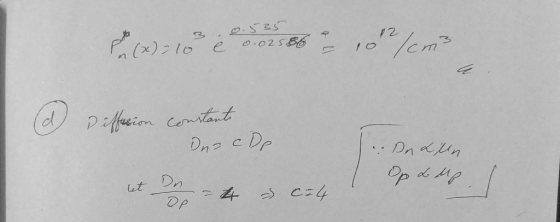
 Problem 3: pn Junction -- Carrier Concentration Profiles The steady-state carrier concentrations inside a Si pn step junction diode maintained at room temperature are shown in the plot below: п or p (log scale Pp -106 10 102 a) Is the diode forward or reverse biased? Explain briefly. b) Do low-level injection conditions prevail in the quasi-neutral regions of the diode? Explain briefly. c) What are the p-side and n-side net dopant concentrations NA and ND, respectively? d) Determine the...
Problem 4 (25 points) Consider a silicon pn junction at T-300 K, NA-ND- 1x101° cm3. The minority ...
 Problem 4 (25 points) Consider a silicon pn junction at T-300 K, NA-ND- 1x101° cm3. The minority carrier lifetimes are τ n-0.01 μs and τ p-0.01 us. The junction is forwardbiased with Va 0.6V. The minority carrier diffusion coefficients are Dn-20 cm s, Dp 10 cm Is. n.-1.5x 1010 cm-3 Depletion region n-type p-type a) (10 points) Calculate the excess electron concentration as a function of x in the p side (see the figure above). b) (5 points) Calculate the...
3. An ideal Si pn junction at 300 K is under forward bias. The minority carrier...
 3. An ideal Si pn junction at 300 K is under forward bias. The minority carrier life times are 10* and 107 s for electrons and holes. The doping concentration in the n-region is ND-10° cmPlot the ratio of hole current to the total current crossing the space charge region as the p-region doping concentration (NA varies over the range 1014 to 1018 cnm Use a log scale for the doping concentrations.[use Fig.3.5(a) on P80 for mobility values) 163 cm....
Problem 4 (25 points) Consider a silicon pn junction at T-300 K, NA-ND- 1x101° cm3. The minority ...
 Can someone help solve this question step by step? Thanks!
Problem 4 (25 points) Consider a silicon pn junction at T-300 K, NA-ND- 1x101° cm3. The minority carrier lifetimes are τ n-0.01 μs and τ p-0.01 us. The junction is forwardbiased with Va 0.6V. The minority carrier diffusion coefficients are Dn-20 cm s, Dp 10 cm Is. n.-1.5x 1010 cm-3 Depletion region n-type p-type a) (10 points) Calculate the excess electron concentration as a function of x in the p...
Can someone help solve this question step by step? Thanks!
Problem 4 (25 points) Consider a silicon pn junction at T-300 K, NA-ND- 1x101° cm3. The minority carrier lifetimes are τ n-0.01 μs and τ p-0.01 us. The junction is forwardbiased with Va 0.6V. The minority carrier diffusion coefficients are Dn-20 cm s, Dp 10 cm Is. n.-1.5x 1010 cm-3 Depletion region n-type p-type a) (10 points) Calculate the excess electron concentration as a function of x in the p...
 this is a problem of semiconductor device and
fundamentals.
Problem 4: pn Junction Current Distributions Consider a Si pn step junction diode maintained at room temperature, with p-side and n-side dopant concentrations NA 1016 cm3 and Np-2x1016 cm3, respectively. (You may assume that each side is uncompensated.) The minority carrier recombination lifetimes are τ,-10-6 s and τ,-10-7 s on the p-side and n-side, respectively a) Calculate the minority carrier densities at the edges of the depletion region when the applied...
this is a problem of semiconductor device and
fundamentals.
Problem 4: pn Junction Current Distributions Consider a Si pn step junction diode maintained at room temperature, with p-side and n-side dopant concentrations NA 1016 cm3 and Np-2x1016 cm3, respectively. (You may assume that each side is uncompensated.) The minority carrier recombination lifetimes are τ,-10-6 s and τ,-10-7 s on the p-side and n-side, respectively a) Calculate the minority carrier densities at the edges of the depletion region when the applied...
 XXX is 467
Design an ideal abrupt silicon PN-junction at 300 K such that the donor impurity concentration in the n-side N, = 5x1015 cm3 and the acceptor impurity concentration in the p-side N, = XXX × 1015/cm3 Assume that the diode area A-2x10⁻³ cm2 and 100cm work Note that the values obtained in the calculations may not be realistic as the Matric # varies greatly. The assignment is only to test your understanding, and must be handwritten Determine the...
XXX is 467
Design an ideal abrupt silicon PN-junction at 300 K such that the donor impurity concentration in the n-side N, = 5x1015 cm3 and the acceptor impurity concentration in the p-side N, = XXX × 1015/cm3 Assume that the diode area A-2x10⁻³ cm2 and 100cm work Note that the values obtained in the calculations may not be realistic as the Matric # varies greatly. The assignment is only to test your understanding, and must be handwritten Determine the...
 Ecp 4.20P) The figure shows ban diagram of a Si PN junction diode. Before solution choose suitable values of a,b and c and show this numbers clearly in a box. a) Calculate the carrier densities plot across the junction (n=1.5 100) b)If you apply reverse bias of 1 V how the carrier densities will change across the junction ?Calculate and plot. Icev Eip- - I a ev Ecn Evp -1 beva EF Ein Eva
 E 4.20P) The figure shows ban diagram of a Si PN junction diode. Before solution choose suitable values of a,b and c and show this numbers clearly in a box. a) Calculate the carrier densities plot across the junction (n=1.5 1019 b)If you apply reverse bias of 1 V how the carrier densities will change across the junction Calculate and plot. ceV Ey- Evp I aev -1 beva En EF En Ev
 Problem 3: pn Junction -- Carrier Concentration Profiles The steady-state carrier concentrations inside a Si pn step junction diode maintained at room temperature are shown in the plot below: п or p (log scale Pp -106 10 102 a) Is the diode forward or reverse biased? Explain briefly. b) Do low-level injection conditions prevail in the quasi-neutral regions of the diode? Explain briefly. c) What are the p-side and n-side net dopant concentrations NA and ND, respectively? d) Determine the...
 Problem 4 (25 points) Consider a silicon pn junction at T-300 K, NA-ND- 1x101° cm3. The minority carrier lifetimes are τ n-0.01 μs and τ p-0.01 us. The junction is forwardbiased with Va 0.6V. The minority carrier diffusion coefficients are Dn-20 cm s, Dp 10 cm Is. n.-1.5x 1010 cm-3 Depletion region n-type p-type a) (10 points) Calculate the excess electron concentration as a function of x in the p side (see the figure above). b) (5 points) Calculate the...
 3. An ideal Si pn junction at 300 K is under forward bias. The minority carrier life times are 10* and 107 s for electrons and holes. The doping concentration in the n-region is ND-10° cmPlot the ratio of hole current to the total current crossing the space charge region as the p-region doping concentration (NA varies over the range 1014 to 1018 cnm Use a log scale for the doping concentrations.[use Fig.3.5(a) on P80 for mobility values) 163 cm....
 Can someone help solve this question step by step? Thanks!
Problem 4 (25 points) Consider a silicon pn junction at T-300 K, NA-ND- 1x101° cm3. The minority carrier lifetimes are τ n-0.01 μs and τ p-0.01 us. The junction is forwardbiased with Va 0.6V. The minority carrier diffusion coefficients are Dn-20 cm s, Dp 10 cm Is. n.-1.5x 1010 cm-3 Depletion region n-type p-type a) (10 points) Calculate the excess electron concentration as a function of x in the p...
Can someone help solve this question step by step? Thanks!
Problem 4 (25 points) Consider a silicon pn junction at T-300 K, NA-ND- 1x101° cm3. The minority carrier lifetimes are τ n-0.01 μs and τ p-0.01 us. The junction is forwardbiased with Va 0.6V. The minority carrier diffusion coefficients are Dn-20 cm s, Dp 10 cm Is. n.-1.5x 1010 cm-3 Depletion region n-type p-type a) (10 points) Calculate the excess electron concentration as a function of x in the p...
Most questions answered within 3 hours.
-
The free energy change for the following reaction at 25 °C, when
[Sn2+] = 1.17 M...
asked 18 minutes ago -
An MNE is this kind of industry when competition in one country
is essentially independent of...
asked 1 hour ago -
. For this set of questions, determine what
proportion of a normal distribution is located betweeneach...
asked 2 hours ago -
A college student is employed as a door-to-door newspaper
salesman. Historical data suggests that the student...
asked 3 hours ago -
MATLAB HW 11 problem using Switch Case and Input commands
Write a script file that calculates...
asked 3 hours ago -
Considering gravitational time dilation, calculate the time that
passes in Earth’s surface while 1 hour passes...
asked 3 hours ago -
Minitab Problem: Take the Lake Hume June rainfall data and find
use the processes outlined in...
asked 4 hours ago -
X Company is trying to decide whether to continue using old
equipment to make Product A...
asked 4 hours ago -
IN PYTHON ONLY !! Program 2: Re-work
program #5 (WeeklyHours) from the previous assignment such that...
asked 5 hours ago -
The average length of time between arrivals at a turnpike
toll-booth is 26 seconds. What is...
asked 6 hours ago -
(a) A piston at 6.1 atm contains a gas that occupies a volume of
3.5 L....
asked 8 hours ago -
Please answer true or false. Words
cannot be changed or added in to make it true...
asked 8 hours ago