
Homework Answers


Add Answer to:
3. (40 pts) The capacitance of a silicon pn junction diode with an area 10° cm2 is measured. A pl...
Problem 4: Schottky Diode-Small-Signal Capacitance Consider the following reverse-bias capacitanc...
 All needed data is given. Please solve the problem ( CLEARLY
)
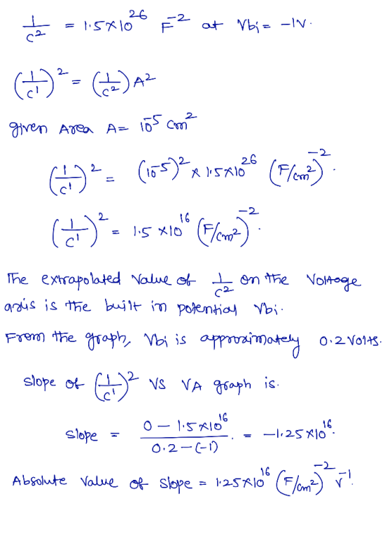
Problem 4: Schottky Diode-Small-Signal Capacitance Consider the following reverse-bias capacitance data for a Schottky diode (n-type silicon) 41/c 12 106 4 22 VA (volts) Given the Area-1.5 X 10⁻³ cm2, find Vbi, No, DBN and the ideal metal work function.
Problem 4: Schottky Diode-Small-Signal Capacitance Consider the following reverse-bias capacitance data for a Schottky diode (n-type silicon) 41/c 12 106 4 22 VA (volts) Given the Area-1.5 X...
All needed data is given. Please solve the problem ( CLEARLY
)
Problem 4: Schottky Diode-Small-Signal Capacitance Consider the following reverse-bias capacitance data for a Schottky diode (n-type silicon) 41/c 12 106 4 22 VA (volts) Given the Area-1.5 X 10⁻³ cm2, find Vbi, No, DBN and the ideal metal work function.
Problem 4: Schottky Diode-Small-Signal Capacitance Consider the following reverse-bias capacitance data for a Schottky diode (n-type silicon) 41/c 12 106 4 22 VA (volts) Given the Area-1.5 X...
Problem 1: Schottky Diode Small-Signal Capacitance Consider the measured reverse-bias capacitance data in Figure 14.8b of...
 Problem 1: Schottky Diode Small-Signal Capacitance Consider the measured reverse-bias capacitance data in Figure 14.8b of Pierret, reproduced below 1/c2 4 103 3. Pp2 -12 10 8 6 4 VA (volts) Illustrate with simple quantitative sketches how the measured curve would change if a) the Schottky barrier Dn decreases to 0.5 eV (but the semiconductor doping concentration remains N-1x10¹⁶ em) b) the semiconductor doping concentration Np increases to 1x1017 cm3 (but the Schottky barrier remains 0.8 eV)
Problem 1: Schottky...
Problem 1: Schottky Diode Small-Signal Capacitance Consider the measured reverse-bias capacitance data in Figure 14.8b of Pierret, reproduced below 1/c2 4 103 3. Pp2 -12 10 8 6 4 VA (volts) Illustrate with simple quantitative sketches how the measured curve would change if a) the Schottky barrier Dn decreases to 0.5 eV (but the semiconductor doping concentration remains N-1x10¹⁶ em) b) the semiconductor doping concentration Np increases to 1x1017 cm3 (but the Schottky barrier remains 0.8 eV)
Problem 1: Schottky...
A silicon PN junction diode is constructed using N-type silicon in which the Fermi level is...
 A silicon PN junction diode is constructed using N-type silicon in which the Fermi level is 100 meV below the conduction band edge and P-type silicon in which the Fermi level is 120 meV above the valence band edge a) What are the majority and minority carrier concentrations on each side of the junction under thermal equilibrium? b) What is the value of the built-in voltage? c) Determine the width of the depletion region on both sides of the junction...
THE REVERSE BIAS VOLTAGE APPLIED TO SILICON PN JUNCTION DIODE IS 4V, DOPING CONCENTRATION Na is...
THE REVERSE BIAS VOLTAGE APPLIED TO SILICON PN JUNCTION DIODE IS 4V, DOPING CONCENTRATION Na is 10^17 cm^-3, Nd = 10^16 cm^-3, ni = 1.3 x 10^9 cm^-3, temperature T = 273 k find the width of depletion region with the applied reverse voltage please check your answer that it is correct please it is a humble request
For an abrupt p-n junction of Area = 10-4 cm2, the measured capacitance under reverse bias...
For an abrupt p-n junction of Area = 10-4 cm2, the measured capacitance under reverse bias of 20 V is 12 pF/cm2. Calculate the donor concentration.
2. (60 pts) Consider a one-sided silicon PN diode. The p-side is degenerately doped (and you...
 2. (60 pts) Consider a one-sided silicon PN diode. The p-side is degenerately doped (and you can assume Ep = Ey for simplicity). The doping concentration on the n-side is Np for 0<x <too. The depletion width on the n-side is xn. Use the depletion approximation. p* ND x 0 From here, you assume that Np is given by 4x1015 cm. (h) (7 pts) What is the maximum electric field in depletion region when Va=-3 V? (i) (8 pts) As...
Design an ideal abrupt silicon PN-junction at 300 K such that the donor impurity concentration in...
 XXX is 467
Design an ideal abrupt silicon PN-junction at 300 K such that the donor impurity concentration in the n-side N, = 5x1015 cm3 and the acceptor impurity concentration in the p-side N, = XXX × 1015/cm3 Assume that the diode area A-2x10⁻³ cm2 and 100cm work Note that the values obtained in the calculations may not be realistic as the Matric # varies greatly. The assignment is only to test your understanding, and must be handwritten Determine the...
XXX is 467
Design an ideal abrupt silicon PN-junction at 300 K such that the donor impurity concentration in the n-side N, = 5x1015 cm3 and the acceptor impurity concentration in the p-side N, = XXX × 1015/cm3 Assume that the diode area A-2x10⁻³ cm2 and 100cm work Note that the values obtained in the calculations may not be realistic as the Matric # varies greatly. The assignment is only to test your understanding, and must be handwritten Determine the...
Problem 4: An abrupt silicon p-n junction diode has the following characteristics. side n-side N-4x 1016cm N1016cm3 n 1000 cm2/V sec 350 cm2/V sec Area A 102cm2 Calculate the following quantities...
 Problem 4: An abrupt silicon p-n junction diode has the following characteristics. side n-side N-4x 1016cm N1016cm3 n 1000 cm2/V sec 350 cm2/V sec Area A 102cm2 Calculate the following quantities: (a) Reverse saturation hole current component (b) Reverse saturation electron current component. (c) Minority carrier concentrations at the edge of the depletion layer, p(0) and pr(0), for a forward voltage of 0.6 V (d) Electron and hole current for the bias condition of (c). (e) Make a rough sketch...
Consider a silicon pn step junction diode with NA-1x1018 cm3 and No 1x1017cm-3, maintained at T...
 Consider a silicon pn step junction diode with NA-1x1018 cm3 and No 1x1017cm-3, maintained at T 300K. The minority carrier lifetimes in the p-side and n-side are τη-10-8 s and Tp-10-7 s, respectively. a) Calculate the minority carrier densities at the edges of the depletion region when the applied voltage (VA) is 0.6 V. of the junction, for the applied bias voltage of part (a) densities are equal in magnitude, for the applied voltage of part (a). b) Sketch the...
consider a silicon pn junction diode at 300 K with nd= na = 10^16 cm-3, u_n 1350 cm^2/v-s, u_p 480 cm^2/v-s, and t_no = t_po= 5×10^-7 s. consider two bias conditions: i) a reverse bias of 1.0 v ii) a...
consider a silicon pn junction diode at 300 K with nd= na = 10^16 cm-3, u_n 1350 cm^2/v-s, u_p 480 cm^2/v-s, and t_no = t_po= 5×10^-7 s. consider two bias conditions: i) a reverse bias of 1.0 v ii) a forward bias of 0.2 v a) for each bus condition, roughly sketch the band gap diagram - accurately label the energy gap in eV - indicate the difference between E_f on the two sides id the junction and label its...
 All needed data is given. Please solve the problem ( CLEARLY
)
Problem 4: Schottky Diode-Small-Signal Capacitance Consider the following reverse-bias capacitance data for a Schottky diode (n-type silicon) 41/c 12 106 4 22 VA (volts) Given the Area-1.5 X 10⁻³ cm2, find Vbi, No, DBN and the ideal metal work function.
Problem 4: Schottky Diode-Small-Signal Capacitance Consider the following reverse-bias capacitance data for a Schottky diode (n-type silicon) 41/c 12 106 4 22 VA (volts) Given the Area-1.5 X...
All needed data is given. Please solve the problem ( CLEARLY
)
Problem 4: Schottky Diode-Small-Signal Capacitance Consider the following reverse-bias capacitance data for a Schottky diode (n-type silicon) 41/c 12 106 4 22 VA (volts) Given the Area-1.5 X 10⁻³ cm2, find Vbi, No, DBN and the ideal metal work function.
Problem 4: Schottky Diode-Small-Signal Capacitance Consider the following reverse-bias capacitance data for a Schottky diode (n-type silicon) 41/c 12 106 4 22 VA (volts) Given the Area-1.5 X...
 Problem 1: Schottky Diode Small-Signal Capacitance Consider the measured reverse-bias capacitance data in Figure 14.8b of Pierret, reproduced below 1/c2 4 103 3. Pp2 -12 10 8 6 4 VA (volts) Illustrate with simple quantitative sketches how the measured curve would change if a) the Schottky barrier Dn decreases to 0.5 eV (but the semiconductor doping concentration remains N-1x10¹⁶ em) b) the semiconductor doping concentration Np increases to 1x1017 cm3 (but the Schottky barrier remains 0.8 eV)
Problem 1: Schottky...
Problem 1: Schottky Diode Small-Signal Capacitance Consider the measured reverse-bias capacitance data in Figure 14.8b of Pierret, reproduced below 1/c2 4 103 3. Pp2 -12 10 8 6 4 VA (volts) Illustrate with simple quantitative sketches how the measured curve would change if a) the Schottky barrier Dn decreases to 0.5 eV (but the semiconductor doping concentration remains N-1x10¹⁶ em) b) the semiconductor doping concentration Np increases to 1x1017 cm3 (but the Schottky barrier remains 0.8 eV)
Problem 1: Schottky...
 A silicon PN junction diode is constructed using N-type silicon in which the Fermi level is 100 meV below the conduction band edge and P-type silicon in which the Fermi level is 120 meV above the valence band edge a) What are the majority and minority carrier concentrations on each side of the junction under thermal equilibrium? b) What is the value of the built-in voltage? c) Determine the width of the depletion region on both sides of the junction...
 2. (60 pts) Consider a one-sided silicon PN diode. The p-side is degenerately doped (and you can assume Ep = Ey for simplicity). The doping concentration on the n-side is Np for 0<x <too. The depletion width on the n-side is xn. Use the depletion approximation. p* ND x 0 From here, you assume that Np is given by 4x1015 cm. (h) (7 pts) What is the maximum electric field in depletion region when Va=-3 V? (i) (8 pts) As...
 XXX is 467
Design an ideal abrupt silicon PN-junction at 300 K such that the donor impurity concentration in the n-side N, = 5x1015 cm3 and the acceptor impurity concentration in the p-side N, = XXX × 1015/cm3 Assume that the diode area A-2x10⁻³ cm2 and 100cm work Note that the values obtained in the calculations may not be realistic as the Matric # varies greatly. The assignment is only to test your understanding, and must be handwritten Determine the...
XXX is 467
Design an ideal abrupt silicon PN-junction at 300 K such that the donor impurity concentration in the n-side N, = 5x1015 cm3 and the acceptor impurity concentration in the p-side N, = XXX × 1015/cm3 Assume that the diode area A-2x10⁻³ cm2 and 100cm work Note that the values obtained in the calculations may not be realistic as the Matric # varies greatly. The assignment is only to test your understanding, and must be handwritten Determine the...
 Problem 4: An abrupt silicon p-n junction diode has the following characteristics. side n-side N-4x 1016cm N1016cm3 n 1000 cm2/V sec 350 cm2/V sec Area A 102cm2 Calculate the following quantities: (a) Reverse saturation hole current component (b) Reverse saturation electron current component. (c) Minority carrier concentrations at the edge of the depletion layer, p(0) and pr(0), for a forward voltage of 0.6 V (d) Electron and hole current for the bias condition of (c). (e) Make a rough sketch...
 Consider a silicon pn step junction diode with NA-1x1018 cm3 and No 1x1017cm-3, maintained at T 300K. The minority carrier lifetimes in the p-side and n-side are τη-10-8 s and Tp-10-7 s, respectively. a) Calculate the minority carrier densities at the edges of the depletion region when the applied voltage (VA) is 0.6 V. of the junction, for the applied bias voltage of part (a) densities are equal in magnitude, for the applied voltage of part (a). b) Sketch the...
Most questions answered within 3 hours.
-
Question Three
Suppose you as project manager are using the Waterfall
development methodology on a large...
asked 51 minutes ago -
Which statement is not true about welfare in Canada?
A.Benefits typically vary based on one's ability...
asked 1 hour ago -
Please help me with FLOWCHART and UML diagram for class,
thank you!
#include <iostream>
#include <fstream>...
asked 2 hours ago -
3. Describe the “logic circuit” of the Lac operon. Which
proteins are bound or not to...
asked 2 hours ago -
Ayesha’s adjusted gross income is $60,000 in 2019. She donated a
piece of artwork with a...
asked 2 hours ago -
For Dijkstra’s shortest path algorithm:
a. Give the Big-O time for Dijkstra’s shortest path algorithm
and...
asked 2 hours ago -
Phosphorus violates the 'octet rule' in biological molecules,
forming more covalent bonds than expected based on...
asked 2 hours ago -
A 1.3 eV electron has a 10-4 probability of tunneling
through a 2.4 eV potential barrier....
asked 2 hours ago -
What is the one ingredient that is common to being successful
with all stakeholders?
profit
trust...
asked 2 hours ago -
Write an assembly language 32 bit program that reads in lines of
text by a .txt...
asked 2 hours ago -
what is the density ( in g/L) of hydrogen gas at 29 degrees C and a...
asked 3 hours ago -
5-6. You are considering three investment alternatives for some
spare cash: Old Reliable Corporation stock (A1),...
asked 2 hours ago