
Homework Answers
Add Answer to:
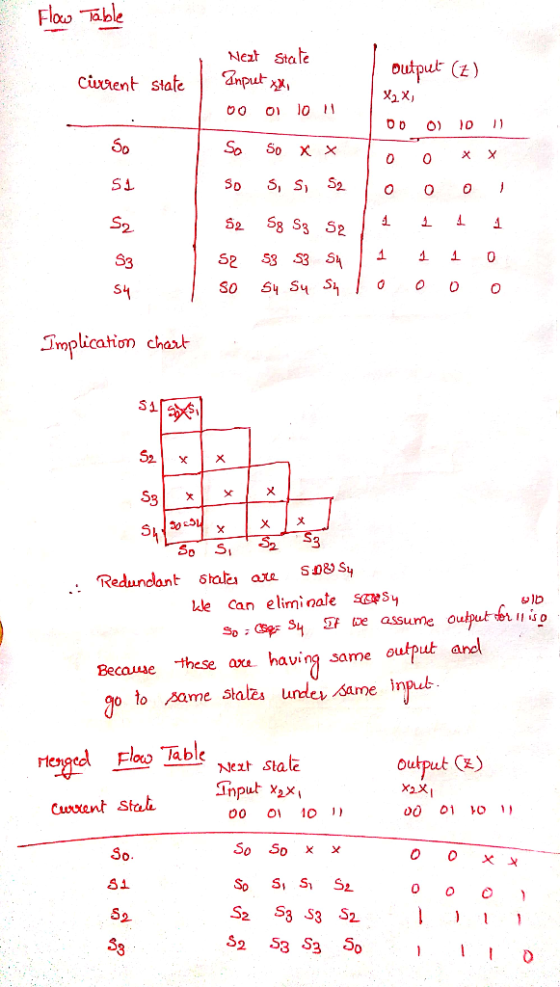
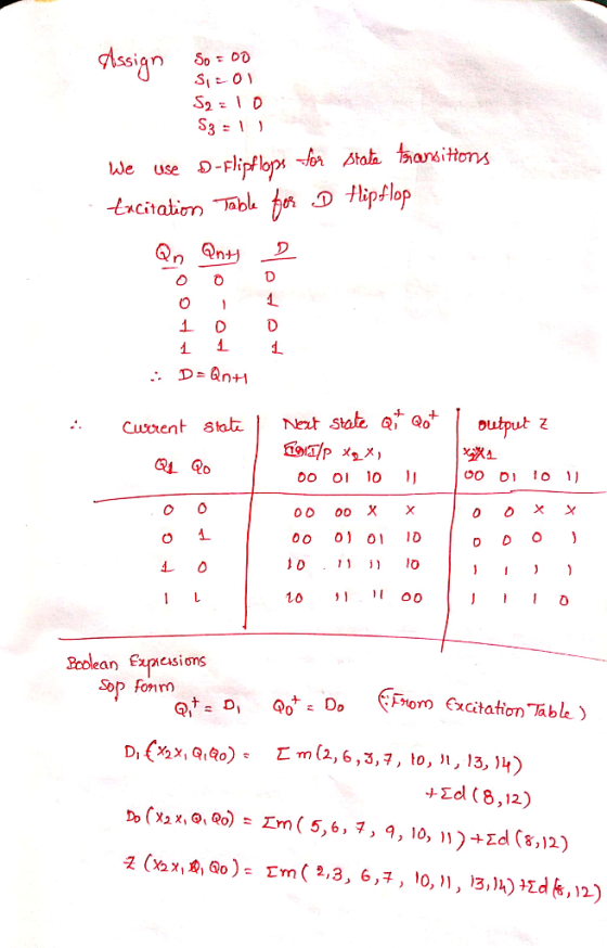
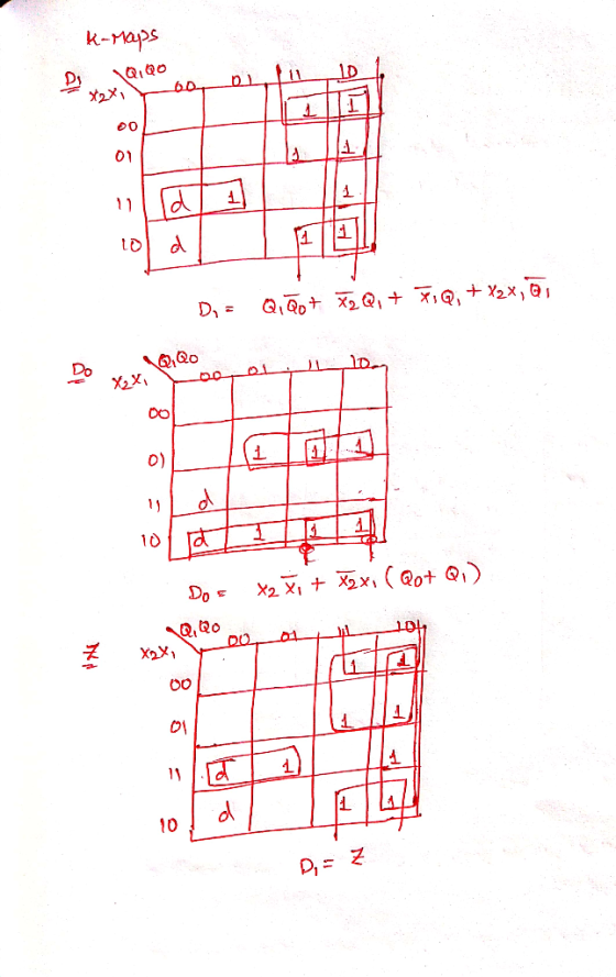
Q3. Figure 3 below shows the initial state diagram for a two input (X2, Xi), single output (Z) control system. Design a...
The state diagram for a sequential circuit in shown below. Input X, Y Output Z 000,D...
 The state diagram for a sequential circuit in shown below. Input X, Y Output Z 000,D 10/0, 11/0 01/1,11/0 00/0,01/0 01/1,10/1 00/1, 10/0 00/1, 11/1 10/0, 11/1 a) b) c) (4 pts) Find the state table (1 pt) Make a state assignment (3 pts) Find an optimized circuit implementation using SR FFs, NAND gates, and inverters.
1. Given the state diagram shown below for a two-state synchronous sequential Mealy circuit with input....
 1. Given the state diagram shown below for a two-state synchronous sequential Mealy circuit with input. and output z, realize the circuit using D flip-flops. Your answer must include the state transition,excita- tion, and output tables, the excitation equation(s), and a labeled circuit diagram 1/0 2. Given the state diagram in Problem 1, realize the circuit using JK flip-flops. Your answer must include the state transition, excitation, and output tables, the excitation equation(s), and a labeled circuit diagram. 3. Given...
1. FSM design. Design a clocked synchronous state machine with one input X, and an output...
 1. FSM design. Design a clocked synchronous state machine with one input X, and an output Z. Z is 1 if 010 sequence pattern has occurred in the input X Otherwise, the output should be 0 For solution: a) Draw the state diagram. b) Write the state/output table. xcitation eqations and output equatio You do not have to draw the circuit diagram. Hint: Three states are needed (two D flip-flops) A: initial state waiting for a 0' from X B:...
SEQUENCE is 101 In Lab Procedure 1. Draw the state diagram of the state machine below...
 SEQUENCE is 101
In Lab Procedure
1. Draw the state diagram of the state machine below and show it
to the lab instructor.
2. Fill the state table.
3. Assign State numbers
4. Find simplified Expressions (State Equations) for the
flip-flops
5. Draw the circuit diagram using NAND GATES ONLY for the state
machine
STATE DIAGRAM::
STATE TABLE::
State Table Next State Qc Y DA DB Dc Present State QA Qв 0 0 0 0 0 0 0 0 0...
SEQUENCE is 101
In Lab Procedure
1. Draw the state diagram of the state machine below and show it
to the lab instructor.
2. Fill the state table.
3. Assign State numbers
4. Find simplified Expressions (State Equations) for the
flip-flops
5. Draw the circuit diagram using NAND GATES ONLY for the state
machine
STATE DIAGRAM::
STATE TABLE::
State Table Next State Qc Y DA DB Dc Present State QA Qв 0 0 0 0 0 0 0 0 0...
9. Product State Graph ou are asked to design a sequence detector to detect the input codes 10 and 01. The input of the circuit is and the output is Z, which only changes at a clock edge. Overla...
 9. Product State Graph ou are asked to design a sequence detector to detect the input codes 10 and 01. The input of the circuit is and the output is Z, which only changes at a clock edge. Overlaps must also be detected. Z only changes at the clock edge . [2%] A. Restate the problem by circling the most appropriate term within the parentheses 1. The circuilt type is (combinational- asynchronous- FSM). 2. The subcategory of the circuit is...
A Moore sequential circuit Y has two inputs (Xi and X2) and one output (Z). Z begins at 0. It becomes 1 when X1 = 1 and X2 = 1 either concurrently, or one after the other (in either order).
 A Moore sequential circuit Y has two inputs (Xi and X2) and one output (Z). Z begins at 0. It becomes 1 when X1 = 1 and X2 = 1 either concurrently, or one after the other (in either order). Z returns to zero when X1= X2 = 0. The following input and output sequences should help you understand the requirements: X1= 01001000110110 X2 = 00110011000100 Z = (0) 00111000110110 (Hint: Y has 4 states and you may consider defining the 4 states with...
ercise 5 Part One: Sequential Logic ask 5.1,1: Design a 4-bit up/down counter that does not...
 ercise 5 Part One: Sequential Logic ask 5.1,1: Design a 4-bit up/down counter that does not overflow or underflow. That is, counting up is disabled when it reaches its maximum value and counting down is disabled when it reaches its minimum value. Use circuit simulation to verify your design. Task 5.1.2: Design a logic implementation of the Finite State Machine in Fiqure 2.3 using JK flip flops. It can be assumed that unused state combinations may be considered as don't...
Given the following State Diagram, write the equations for the D-Flipflop A, D-Flipflop B, and Output....
 Given the following State Diagram, write the equations for the
D-Flipflop A,
D-Flipflop B, and Output. Please enter the equations in the space
provided.
11/0 АВ 00 XҮ/Z 01/1 11/0 00/1 01/1, 10/0 00/0, 01/0, 10/0 10 01 00/0 11/1 11/1 10/1 01/1, 10/1 11 00/0 A B
Given the following State Diagram, write the equations for the
D-Flipflop A,
D-Flipflop B, and Output. Please enter the equations in the space
provided.
11/0 АВ 00 XҮ/Z 01/1 11/0 00/1 01/1, 10/0 00/0, 01/0, 10/0 10 01 00/0 11/1 11/1 10/1 01/1, 10/1 11 00/0 A B
Thc state transition table bclow is for a sequential circuit with onc input X and onc output Y. The circuit has two state variables A and B, and synchronous input Reset that resets the circuit to sta...
 Thc state transition table bclow is for a sequential circuit with onc input X and onc output Y. The circuit has two state variables A and B, and synchronous input Reset that resets the circuit to state AB-01 when Reset 1: Present State Next State Output X-0 A B A B 0 Reset State 0 0 (9 points) Implement the sequential circuit using minimum number of logic gates and rising- edge triggered D-FFs and draw the logic diagram of the...
show work plz Consider the following finite state diagram. State 1 Output=1 State 0 Output=0 State...
 show work plz
Consider the following finite state diagram. State 1 Output=1 State 0 Output=0 State 2 Output=1 State 3 Output=0 The diagram has 4 states, 1 external input / (in additional to the CLK input), and 1 output bit Y. State 0 is represented by memory bits Qi Qo=00, State 1 is represented by memory bits Q.Qo=01, State 2 is represented by memory bits Q.Qo = 10, and State 3 is represented by memory bits Q.Qo = 11. The...
show work plz
Consider the following finite state diagram. State 1 Output=1 State 0 Output=0 State 2 Output=1 State 3 Output=0 The diagram has 4 states, 1 external input / (in additional to the CLK input), and 1 output bit Y. State 0 is represented by memory bits Qi Qo=00, State 1 is represented by memory bits Q.Qo=01, State 2 is represented by memory bits Q.Qo = 10, and State 3 is represented by memory bits Q.Qo = 11. The...
 The state diagram for a sequential circuit in shown below. Input X, Y Output Z 000,D 10/0, 11/0 01/1,11/0 00/0,01/0 01/1,10/1 00/1, 10/0 00/1, 11/1 10/0, 11/1 a) b) c) (4 pts) Find the state table (1 pt) Make a state assignment (3 pts) Find an optimized circuit implementation using SR FFs, NAND gates, and inverters.
 1. Given the state diagram shown below for a two-state synchronous sequential Mealy circuit with input. and output z, realize the circuit using D flip-flops. Your answer must include the state transition,excita- tion, and output tables, the excitation equation(s), and a labeled circuit diagram 1/0 2. Given the state diagram in Problem 1, realize the circuit using JK flip-flops. Your answer must include the state transition, excitation, and output tables, the excitation equation(s), and a labeled circuit diagram. 3. Given...
 1. FSM design. Design a clocked synchronous state machine with one input X, and an output Z. Z is 1 if 010 sequence pattern has occurred in the input X Otherwise, the output should be 0 For solution: a) Draw the state diagram. b) Write the state/output table. xcitation eqations and output equatio You do not have to draw the circuit diagram. Hint: Three states are needed (two D flip-flops) A: initial state waiting for a 0' from X B:...
 SEQUENCE is 101
In Lab Procedure
1. Draw the state diagram of the state machine below and show it
to the lab instructor.
2. Fill the state table.
3. Assign State numbers
4. Find simplified Expressions (State Equations) for the
flip-flops
5. Draw the circuit diagram using NAND GATES ONLY for the state
machine
STATE DIAGRAM::
STATE TABLE::
State Table Next State Qc Y DA DB Dc Present State QA Qв 0 0 0 0 0 0 0 0 0...
SEQUENCE is 101
In Lab Procedure
1. Draw the state diagram of the state machine below and show it
to the lab instructor.
2. Fill the state table.
3. Assign State numbers
4. Find simplified Expressions (State Equations) for the
flip-flops
5. Draw the circuit diagram using NAND GATES ONLY for the state
machine
STATE DIAGRAM::
STATE TABLE::
State Table Next State Qc Y DA DB Dc Present State QA Qв 0 0 0 0 0 0 0 0 0...
 9. Product State Graph ou are asked to design a sequence detector to detect the input codes 10 and 01. The input of the circuit is and the output is Z, which only changes at a clock edge. Overlaps must also be detected. Z only changes at the clock edge . [2%] A. Restate the problem by circling the most appropriate term within the parentheses 1. The circuilt type is (combinational- asynchronous- FSM). 2. The subcategory of the circuit is...
 ercise 5 Part One: Sequential Logic ask 5.1,1: Design a 4-bit up/down counter that does not overflow or underflow. That is, counting up is disabled when it reaches its maximum value and counting down is disabled when it reaches its minimum value. Use circuit simulation to verify your design. Task 5.1.2: Design a logic implementation of the Finite State Machine in Fiqure 2.3 using JK flip flops. It can be assumed that unused state combinations may be considered as don't...
 Given the following State Diagram, write the equations for the
D-Flipflop A,
D-Flipflop B, and Output. Please enter the equations in the space
provided.
11/0 АВ 00 XҮ/Z 01/1 11/0 00/1 01/1, 10/0 00/0, 01/0, 10/0 10 01 00/0 11/1 11/1 10/1 01/1, 10/1 11 00/0 A B
Given the following State Diagram, write the equations for the
D-Flipflop A,
D-Flipflop B, and Output. Please enter the equations in the space
provided.
11/0 АВ 00 XҮ/Z 01/1 11/0 00/1 01/1, 10/0 00/0, 01/0, 10/0 10 01 00/0 11/1 11/1 10/1 01/1, 10/1 11 00/0 A B
 Thc state transition table bclow is for a sequential circuit with onc input X and onc output Y. The circuit has two state variables A and B, and synchronous input Reset that resets the circuit to state AB-01 when Reset 1: Present State Next State Output X-0 A B A B 0 Reset State 0 0 (9 points) Implement the sequential circuit using minimum number of logic gates and rising- edge triggered D-FFs and draw the logic diagram of the...
 show work plz
Consider the following finite state diagram. State 1 Output=1 State 0 Output=0 State 2 Output=1 State 3 Output=0 The diagram has 4 states, 1 external input / (in additional to the CLK input), and 1 output bit Y. State 0 is represented by memory bits Qi Qo=00, State 1 is represented by memory bits Q.Qo=01, State 2 is represented by memory bits Q.Qo = 10, and State 3 is represented by memory bits Q.Qo = 11. The...
show work plz
Consider the following finite state diagram. State 1 Output=1 State 0 Output=0 State 2 Output=1 State 3 Output=0 The diagram has 4 states, 1 external input / (in additional to the CLK input), and 1 output bit Y. State 0 is represented by memory bits Qi Qo=00, State 1 is represented by memory bits Q.Qo=01, State 2 is represented by memory bits Q.Qo = 10, and State 3 is represented by memory bits Q.Qo = 11. The...
Most questions answered within 3 hours.
-
Two electrons are initially at rest separated by a distance of
2nm. At time t=0, they...
asked 1 minute ago -
Magnesium and nitrogen react in a combination reaction to
produce magnesium nitride. 3 Mg + N2...
asked 3 minutes ago -
A martial artist is practicing breaking 5 boards. He is able to
break aboard with probability...
asked 8 minutes ago -
The rate constant of a first-order reaction is 2.95 × 10⁻⁴ s−1
at 350.° C. If...
asked 11 minutes ago -
implement a class called PiggyBank that will be used to
represent a collection of coins. Functionality...
asked 2 minutes ago -
2. Use the following information in the table to answer the
following questions. (Numbers are in...
asked 8 minutes ago -
The fuel economy of a 2011 Lexus RX 350 2wd 6 cylinder 3.5 L
automatic 5...
asked 16 minutes ago -
i.
the synthesized compund 2-bromo-butanal i have a IR peak at about
3200 and one at...
asked 16 minutes ago -
A
752 mL sample of water was placed in a 1000 gram pan of aluminum.
The...
asked 27 minutes ago -
1.In the context of chelation, what does binding strength mean?
What happens at the molecular level...
asked 20 minutes ago -
Describe two obstacles that makes fixing atmospheric nitrogen
difficult.
asked 40 minutes ago -
Evelyn incorporates her sole proprietorship, transferring it to
newly formed Papaya Corporation. The assets transferred have...
asked 26 minutes ago