
Homework Answers

Add Answer to:
Q3 A MOSFET is used as a low-side switch to control a 15 2 resistive load...
Please answer all the parts of the question clearly and fully! Thank you! Numerical Answers: (b)...
 Please answer all the parts of the question clearly and fully!
Thank you!
Numerical Answers:
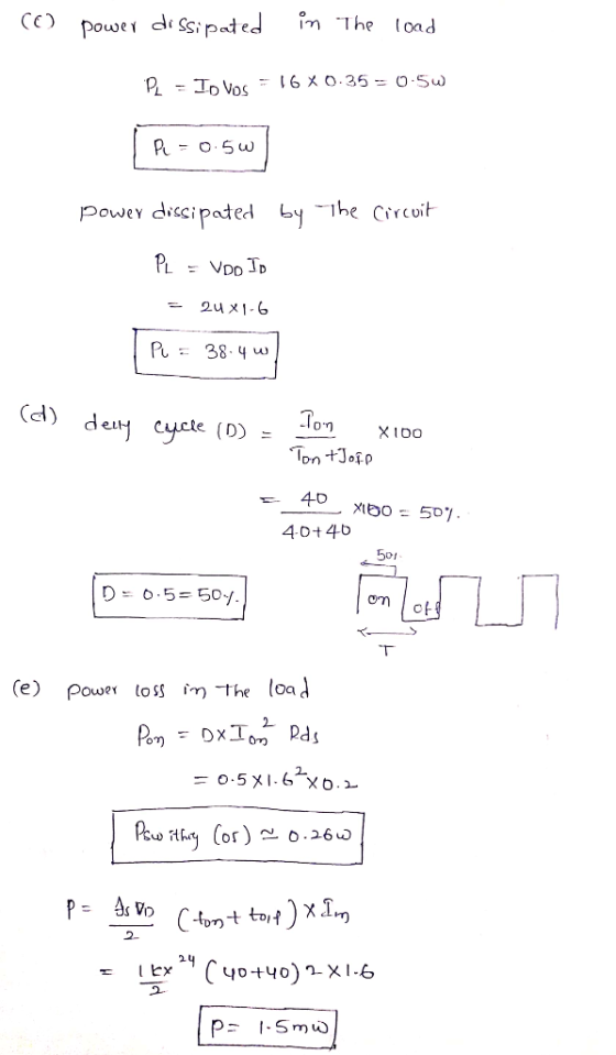
(b) (0.0 A, 24 V), (approximately 1.6 A, 0.32 V)
(c) 38.4 W, 0.5 W
(e) 0.26 W + 1.5 mW
SECTION B: Attempt any Two) questions 150 marks total! Q3 A MOSFET is used as a low-side switch to control a 15 2 resistive load from a 24 supply. The MOSFET has RDSan VDC 0.2 ? and ton-tof-40 ns. (a) Draw a suitable circuit....
Please answer all the parts of the question clearly and fully!
Thank you!
Numerical Answers:
(b) (0.0 A, 24 V), (approximately 1.6 A, 0.32 V)
(c) 38.4 W, 0.5 W
(e) 0.26 W + 1.5 mW
SECTION B: Attempt any Two) questions 150 marks total! Q3 A MOSFET is used as a low-side switch to control a 15 2 resistive load from a 24 supply. The MOSFET has RDSan VDC 0.2 ? and ton-tof-40 ns. (a) Draw a suitable circuit....
A MOSFET and diode is used in a circuit shown in figure. The operating conditions are...
A MOSFET and diode is used in a circuit shown in figure. The operating conditions are as follows: Input Voltage = VIN = 42 V, Io = 5A. Switching frequency fs = 400 kHz, Duty-cycle = D = 0.3. Diode Forward Voltage drop = 0.7V. Diode Peak Reverse Recovery Current = IRRM = 2.5 A. ON-state resistance of the MOSFET is RDS (on) = 25 mΩ. VGG as a step voltage between 0V and 10 V. MOSFET timings – Td...
1. A step-down chopper is connected to a 90VDC source and a 3Ω resistive load. The...
1. A step-down chopper is connected to a 90VDC source and a 3Ω resistive load. The chopper switching frequency is 5kHz with a 40% duty-cycle (D) Average free-wheeling diode current 2. A step-down chopper is connected to a 90VDC source and a 3Ω resistive load. The chopper switching frequency is 5kHz with a 40% duty-cycle (D) Size of inductance for a 10% peak-to-peak current ripple 3. VS = 90V EMF = 40V R = 2Ω L = 10mH switching frequency = 5kHz...
To design a high efficiency d.c., to d.c power converter with the given specifications min 10V max 15V nominal (regulated) 8V Input voltage: Output voltage: Nominal load current: 4A Inductor current...
 To design a high efficiency d.c., to d.c power converter with the given specifications min 10V max 15V nominal (regulated) 8V Input voltage: Output voltage: Nominal load current: 4A Inductor current ripple: 0.1A max Switching frequency: 30 kHz Output voltage ripple: 20 mV Define a suitable power circuit topology to meet the above specification? Sketch a circuit diagram of the chosen power circuit topology (a) Define the minimum and maximum duty cycles assuming that the control circuit keeps the output...
Given: A MOSFET is used in a switching power-pole found in Fig. 2-4a of the text....
 Given: A MOSFET is used in a switching power-pole found in Fig. 2-4a of the text. The operating conditions are as follows: Vin 35V, 6 A, the switching frequency fs 300 kHz, and the duty ratio d 0.4 a) Consider the diode in the power pole. Assuming an offset voltage forward bias model of the free-wheeling diode in which VM 1.2 V, calculate the average forward power loss in the diode HINT: Consider Eq. 2A-1 b) In the diode reverse...
a9a resistive load. Inductor 3-(35 pts) Design a converter that has an input voltage of 24 V DC and supplies 18 V DC to current is desired to be continuous and must not change more than 30 % of i...
 a9a resistive load. Inductor 3-(35 pts) Design a converter that has an input voltage of 24 V DC and supplies 18 V DC to current is desired to be continuous and must not change more than 30 % of its average value voltage ripple must be lower than 2 %. Switching frequency is 10 kHz. a) Draw the circuit diagram. Calculate the duty ratio. Calculate values for 2 desired conditions of the inductor current and determine the value of the...
1. to design a high efficiency d.c. to d.c. power converter with the given specifications Input v...
 1. to design a high efficiency d.c. to d.c. power converter with the given specifications Input voltage Output voltage Nominal load current: 4A Inductor current ripple: 0.1A max Switching frequency: 30 kHz Output voltage ripple: 20 mV min 10V max 15V nominal (regulated) 8V Define a suitable power circuit topology to meet the above specification Sketch a circuit diagram of the chosen power circuit topology (a) Define the minimum and maximum duty cycles assuming that the control circuit keeps the...
Problem 2: Pulse width modulation (PWM) is a method of reducing the average power delivered by...
 Problem 2: Pulse width modulation (PWM) is a method of reducing the average power delivered by an electrical signal, by effectively chopping it up into discrete parts. The average value of voltage fed to the load is controlled by turning the switch between supply and load on and off at a fast rate. The longer the switch is on compared to the off periods, the higher the total power supplied to the load. PWM is particularly suited for running DC...
Design a boost converter power stage to the following specification: Input voltage Output voltage: Output voltage...
 Design a boost converter power stage to the following specification: Input voltage Output voltage: Output voltage ripple:max 20mV Load power: Switching frequency: 15kHz 110-125V 300V 1.5kW Calculate: (i) Maximum duty cycle (ii) Minimum duty cycle (iii) Average diode current (iv) Assuming the Rds(on) of the MOSFET is 0.01 Ω, and the diode forward voltage is 0.8V, calculate the approximate efficiency of the circuit. 2. A switching power supply shown in the circuit below has its switch driven by a signal...
Design a common-source MOSFET amplifier such that RG is a multiple of D = o.st mot...
 Design a common-source MOSFET amplifier such that RG is a multiple of D = o.st mot (Avol 15.02 VN RL = 17kr • Choose a sinusoidal signal voltage, Vsig, with Rsig = 400 kN to use as the input in this problem. Use 2 kHz as the frequency of your sinusoidal. This is a design problem so vsig will not be unique. Use V+ = 0.8 V, k = 5 mA/V2, and VA = 80 V for your MOSFET. Assume...
 Please answer all the parts of the question clearly and fully!
Thank you!
Numerical Answers:
(b) (0.0 A, 24 V), (approximately 1.6 A, 0.32 V)
(c) 38.4 W, 0.5 W
(e) 0.26 W + 1.5 mW
SECTION B: Attempt any Two) questions 150 marks total! Q3 A MOSFET is used as a low-side switch to control a 15 2 resistive load from a 24 supply. The MOSFET has RDSan VDC 0.2 ? and ton-tof-40 ns. (a) Draw a suitable circuit....
Please answer all the parts of the question clearly and fully!
Thank you!
Numerical Answers:
(b) (0.0 A, 24 V), (approximately 1.6 A, 0.32 V)
(c) 38.4 W, 0.5 W
(e) 0.26 W + 1.5 mW
SECTION B: Attempt any Two) questions 150 marks total! Q3 A MOSFET is used as a low-side switch to control a 15 2 resistive load from a 24 supply. The MOSFET has RDSan VDC 0.2 ? and ton-tof-40 ns. (a) Draw a suitable circuit....
 To design a high efficiency d.c., to d.c power converter with the given specifications min 10V max 15V nominal (regulated) 8V Input voltage: Output voltage: Nominal load current: 4A Inductor current ripple: 0.1A max Switching frequency: 30 kHz Output voltage ripple: 20 mV Define a suitable power circuit topology to meet the above specification? Sketch a circuit diagram of the chosen power circuit topology (a) Define the minimum and maximum duty cycles assuming that the control circuit keeps the output...
 Given: A MOSFET is used in a switching power-pole found in Fig. 2-4a of the text. The operating conditions are as follows: Vin 35V, 6 A, the switching frequency fs 300 kHz, and the duty ratio d 0.4 a) Consider the diode in the power pole. Assuming an offset voltage forward bias model of the free-wheeling diode in which VM 1.2 V, calculate the average forward power loss in the diode HINT: Consider Eq. 2A-1 b) In the diode reverse...
 a9a resistive load. Inductor 3-(35 pts) Design a converter that has an input voltage of 24 V DC and supplies 18 V DC to current is desired to be continuous and must not change more than 30 % of its average value voltage ripple must be lower than 2 %. Switching frequency is 10 kHz. a) Draw the circuit diagram. Calculate the duty ratio. Calculate values for 2 desired conditions of the inductor current and determine the value of the...
 1. to design a high efficiency d.c. to d.c. power converter with the given specifications Input voltage Output voltage Nominal load current: 4A Inductor current ripple: 0.1A max Switching frequency: 30 kHz Output voltage ripple: 20 mV min 10V max 15V nominal (regulated) 8V Define a suitable power circuit topology to meet the above specification Sketch a circuit diagram of the chosen power circuit topology (a) Define the minimum and maximum duty cycles assuming that the control circuit keeps the...
 Problem 2: Pulse width modulation (PWM) is a method of reducing the average power delivered by an electrical signal, by effectively chopping it up into discrete parts. The average value of voltage fed to the load is controlled by turning the switch between supply and load on and off at a fast rate. The longer the switch is on compared to the off periods, the higher the total power supplied to the load. PWM is particularly suited for running DC...
 Design a boost converter power stage to the following specification: Input voltage Output voltage: Output voltage ripple:max 20mV Load power: Switching frequency: 15kHz 110-125V 300V 1.5kW Calculate: (i) Maximum duty cycle (ii) Minimum duty cycle (iii) Average diode current (iv) Assuming the Rds(on) of the MOSFET is 0.01 Ω, and the diode forward voltage is 0.8V, calculate the approximate efficiency of the circuit. 2. A switching power supply shown in the circuit below has its switch driven by a signal...
 Design a common-source MOSFET amplifier such that RG is a multiple of D = o.st mot (Avol 15.02 VN RL = 17kr • Choose a sinusoidal signal voltage, Vsig, with Rsig = 400 kN to use as the input in this problem. Use 2 kHz as the frequency of your sinusoidal. This is a design problem so vsig will not be unique. Use V+ = 0.8 V, k = 5 mA/V2, and VA = 80 V for your MOSFET. Assume...
Most questions answered within 3 hours.
-
Evaluate a specific listening situation using the Sapir-Whorf
and Bernstein hypothesis. What was thecontext? What was...
asked 18 seconds from now -
Recall that if X is a Student’s t random variable with n df,
then by definition...
asked 17 minutes ago -
A charge of -2.95 µC is fixed in place. From a horizontal
distance of 0.0470 m,...
asked 14 minutes ago -
Consider the following information:
Your company makes widgets. You are trying to figure out what
volume...
asked 16 minutes ago -
Math 333 Plz help ASAP
The yield of a chemical process is being studied. From previous...
asked 32 minutes ago -
Cobb-Douglas Preferences: Cobb-Douglas preferences on the
consump-
tion set R2+ can be represented by a utility...
asked 28 minutes ago -
In your experience, what are some of the barriers to the
successful implementation of a project?...
asked 31 minutes ago -
1. A normal distribution has a mean of
μ = 60 and a standard deviation
of...
asked 33 minutes ago -
The size of your Social Security benefits is determined by:
(select all that apply) Question 1...
asked 46 minutes ago -
Starch polymers are broken down by enzymes into monomers
called:
a.)maltose
b.) dextrins
c.) glucose
d.)...
asked 52 minutes ago -
How does HA (High Availability) work and name two ways it can
help an organization?
asked 55 minutes ago -
Saginaw Company is a garden products wholesale firm. In
December, Saginaw Company expects to sell 26,000...
asked 55 minutes ago