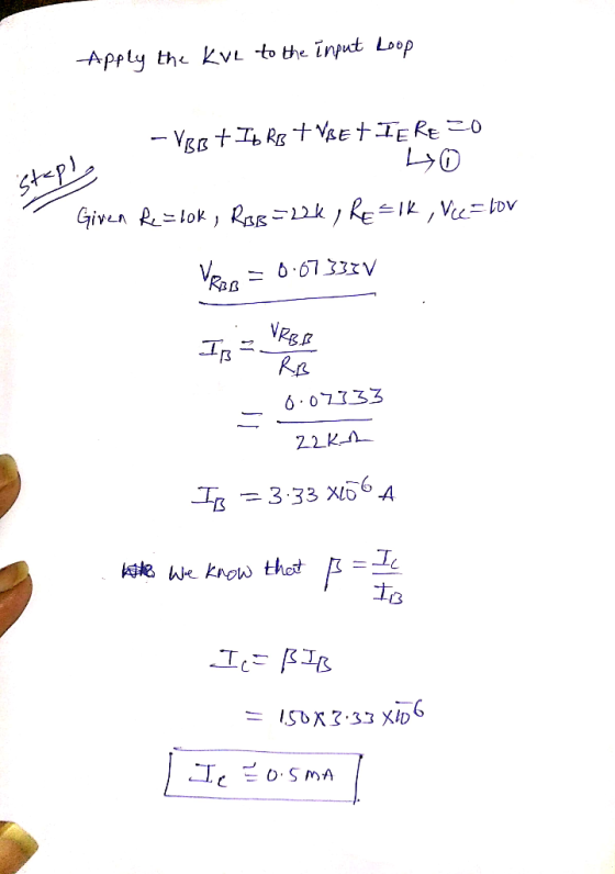
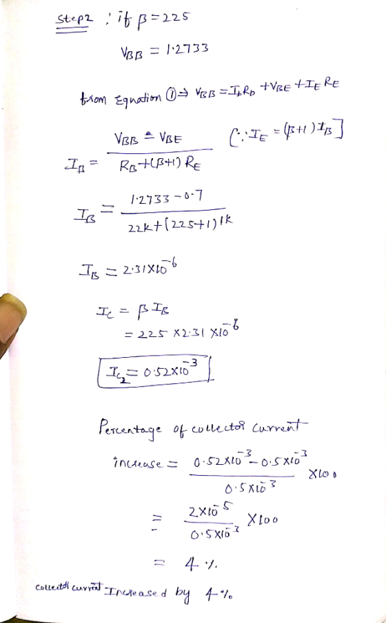
I cropped out Step 1 to only show information that may or may not be vital. I only need help with Step 2. Thank you.

Homework Answers
Add Answer to:
I cropped out Step 1 to only show information that may or may
not be vital....
Please answer clearly 2. Consider the circuit shown in Figure 1. Determine values of Ri, R2, and Rc to provide the quie...
 Please answer clearly
2. Consider the circuit shown in Figure 1. Determine values of Ri, R2, and Rc to provide the quiescent emitter current 1.5 mA and the quiescent collector to emitter voltage 5V. Assume β 100, Re-I㏀、Va= 200V, VBEon-0.7V, and VT= 25mV. R1 Rc Vcc に 10v R2 Re Figure 1: BJT biasing configuration
2. Consider the circuit shown in Figure 1. Determine values of Ri, R2, and Rc to provide the quiescent emitter current 1.5 mA and the...
Please answer clearly
2. Consider the circuit shown in Figure 1. Determine values of Ri, R2, and Rc to provide the quiescent emitter current 1.5 mA and the quiescent collector to emitter voltage 5V. Assume β 100, Re-I㏀、Va= 200V, VBEon-0.7V, and VT= 25mV. R1 Rc Vcc に 10v R2 Re Figure 1: BJT biasing configuration
2. Consider the circuit shown in Figure 1. Determine values of Ri, R2, and Rc to provide the quiescent emitter current 1.5 mA and the...
Q5: In the following circuit, identical diodes Dl and D2 use constant voltage drop (CVD) model....
 Q5: In the following circuit, identical diodes Dl and D2 use constant voltage drop (CVD) model. VD,ON = 800 mV, R1 = 1 K. Determine the change in Vout if Vin changes from +2.4V to +2.5V. (Hint: use small signal model) Vin - DR Nyu out 'out 1K12 z Q6: The following BJT circuit has VBE = 0.8V, VA = 10V, Vcc = 2.5V. The amplifier must be designed for maximum small signal voltage gain Ay, while maintaining Q1 operating...
+10V Analysis Problems R voltage OV out 1) Design the given circuit configuration such that the...
 +10V Analysis Problems R voltage OV out 1) Design the given circuit configuration such that the output voltage -2.4V. Assume that the diodes available to you have a voltage drop of 0.7V across them when flowing a current of ImA. Also, the voltage across these diodes changes by 0.1V for every decade-change-in-the- current through them. Assume identical diodes. 1
Please only use PSpice as stated in the directions. Any other software will not be accepted....
 Please only use PSpice as stated in the directions. Any other
software will not be accepted. Thanks
No multisim or LTSpice.
Part I: Transistor Output Characteristic Procedure: 1. Build the circuit model in PSpice as shown in Fig. 1 with Vbb = 10V, R2 = 330 k92 and R3 = 0.22 k22. R3 0.22 Vec vbь R2 Q1 10V 330k or 147k Figure 1. Circuit configuration for Transistor output characteristic testing 2. Use Ohm's Law to calculate Ib. You may...
Please only use PSpice as stated in the directions. Any other
software will not be accepted. Thanks
No multisim or LTSpice.
Part I: Transistor Output Characteristic Procedure: 1. Build the circuit model in PSpice as shown in Fig. 1 with Vbb = 10V, R2 = 330 k92 and R3 = 0.22 k22. R3 0.22 Vec vbь R2 Q1 10V 330k or 147k Figure 1. Circuit configuration for Transistor output characteristic testing 2. Use Ohm's Law to calculate Ib. You may...
Could someone please help me on how I should be configuring the circuit in Figure 4(a)...
 Could someone please help me on how I should be configuring the
circuit in Figure 4(a) in Multisim? Basically not understanding
question #1 in the Procedure. Cannot keep Vrb the same value while
adjusting Vcc. Then when trying to adjust Vbb to hold Vrb, Ib
changes.
Any help is appreciated!
Discrete Devices Section LAB 4 BJT CHARACTERISTICS AND BIASING Objective: The objective of this laboratory is to examine the operation of a bipolar junction transistor and plot its output characteristics...
Could someone please help me on how I should be configuring the
circuit in Figure 4(a) in Multisim? Basically not understanding
question #1 in the Procedure. Cannot keep Vrb the same value while
adjusting Vcc. Then when trying to adjust Vbb to hold Vrb, Ib
changes.
Any help is appreciated!
Discrete Devices Section LAB 4 BJT CHARACTERISTICS AND BIASING Objective: The objective of this laboratory is to examine the operation of a bipolar junction transistor and plot its output characteristics...
please choose one of the answer choices above. Must show all work, thank you Question 1...
 please choose one of the answer choices above.
Must show all work, thank you
Question 1 CIRCUIT A.1 (2.5 Marks) + Vcc RB IB Rc Vc VB Fig. 1: CIRCUIT A.1 Statement: Sketching relevant output (Vc-Ic) characteristics decide on Q-point coordinates and DC load-line details: That is, determine DC operating conditions of the NPN-BJT/Si circuit of Fig.1 (denoting the type Circuit A1). Assume the following: Vcc= 12 volt; Rc = 3.6 k; RB = 500 k and a = 0.9....
please choose one of the answer choices above.
Must show all work, thank you
Question 1 CIRCUIT A.1 (2.5 Marks) + Vcc RB IB Rc Vc VB Fig. 1: CIRCUIT A.1 Statement: Sketching relevant output (Vc-Ic) characteristics decide on Q-point coordinates and DC load-line details: That is, determine DC operating conditions of the NPN-BJT/Si circuit of Fig.1 (denoting the type Circuit A1). Assume the following: Vcc= 12 volt; Rc = 3.6 k; RB = 500 k and a = 0.9....
4. Lab VIII: Experiment VII The Bipolar Junction Transistor (BJT) Characteristics The bipolar junction transistor (BJT)...
 4. Lab VIII: Experiment VII The Bipolar Junction Transistor (BJT) Characteristics The bipolar junction transistor (BJT) is a three-terminal solid state device widely used as an amplifier (or switching) device. It consists of two n-type materials sandwiched by p-type material (npn) or two p-type and n-type. The terminals (sections) are known as emitter E, base B and collector C. Two currents and two voltages uniquely describe the behavior of the device. The third current/voltage can be determined through KCL/KVL. See...
Fundamentals of Electronic Engineering Answer should be step by step and readable (clear handwriting) Given: •...
 Fundamentals of Electronic Engineering
Answer should be step by step and readable (clear
handwriting)
Given: • Power voltage: • Collector resistor: • Current amplification of BJT: • Source peak voltage: • Input/Output resistance: • The corner frequency: Vcc = 12V; Rc = 4k22; B = 100; Vs = 10mV; Rvs, RL = 1 ks2; f-3dB = 100Hz. Vec=12V w • Rc www R1 HE Сс CC2 RL + R2 RE CE Find: ? Bias quiescent point: Load line, Q-point, VcEQ,...
Fundamentals of Electronic Engineering
Answer should be step by step and readable (clear
handwriting)
Given: • Power voltage: • Collector resistor: • Current amplification of BJT: • Source peak voltage: • Input/Output resistance: • The corner frequency: Vcc = 12V; Rc = 4k22; B = 100; Vs = 10mV; Rvs, RL = 1 ks2; f-3dB = 100Hz. Vec=12V w • Rc www R1 HE Сс CC2 RL + R2 RE CE Find: ? Bias quiescent point: Load line, Q-point, VcEQ,...
please choose one of the answer choices above. Must show all work, thank you Question 2...
 please choose one of the answer choices above.
Must show all work, thank you
Question 2 CIRCUIT A2 (2.5 Marks) + Ver Rc Ic с IR Fig. 2: CIRCUIT A.2 Statement: Sketching relevant output (Vc-Ic) characteristics decide on Q-point coordinates and DC load-line details: That is, determine DC operating conditions of the NPN-BJT/Si circuit of Fig.2 (denoting the type Circuit A2). Assume the following: Vcc= 24 volt; Rc = 5.0 k; RB = 1500 k and B = 125. Required...
please choose one of the answer choices above.
Must show all work, thank you
Question 2 CIRCUIT A2 (2.5 Marks) + Ver Rc Ic с IR Fig. 2: CIRCUIT A.2 Statement: Sketching relevant output (Vc-Ic) characteristics decide on Q-point coordinates and DC load-line details: That is, determine DC operating conditions of the NPN-BJT/Si circuit of Fig.2 (denoting the type Circuit A2). Assume the following: Vcc= 24 volt; Rc = 5.0 k; RB = 1500 k and B = 125. Required...
please choose one of the answer choices above. Must show all work, thank you Question 4...
 please choose one of the answer choices above.
Must show all work, thank you
Question 4 CIRCUIT B2 (2.5 Marks) +Vcc Rc IRC Vic RB Ів Vc VB VE RE IE FIG.4: CIRCUIT B2 Statement: Sketching relevant output (Vc-Ic) characteristics decide on Q-point coordinates and DC load-line details: That is, determine DC operating conditions of the NPN-BJT/Si circuit of Fig.4 (denoting the type Circuit B2). Assume the following: Vcc= 24 volt; Rc = 5.0 k; RE = 1000 ohm; RB...
please choose one of the answer choices above.
Must show all work, thank you
Question 4 CIRCUIT B2 (2.5 Marks) +Vcc Rc IRC Vic RB Ів Vc VB VE RE IE FIG.4: CIRCUIT B2 Statement: Sketching relevant output (Vc-Ic) characteristics decide on Q-point coordinates and DC load-line details: That is, determine DC operating conditions of the NPN-BJT/Si circuit of Fig.4 (denoting the type Circuit B2). Assume the following: Vcc= 24 volt; Rc = 5.0 k; RE = 1000 ohm; RB...
 Please answer clearly
2. Consider the circuit shown in Figure 1. Determine values of Ri, R2, and Rc to provide the quiescent emitter current 1.5 mA and the quiescent collector to emitter voltage 5V. Assume β 100, Re-I㏀、Va= 200V, VBEon-0.7V, and VT= 25mV. R1 Rc Vcc に 10v R2 Re Figure 1: BJT biasing configuration
2. Consider the circuit shown in Figure 1. Determine values of Ri, R2, and Rc to provide the quiescent emitter current 1.5 mA and the...
Please answer clearly
2. Consider the circuit shown in Figure 1. Determine values of Ri, R2, and Rc to provide the quiescent emitter current 1.5 mA and the quiescent collector to emitter voltage 5V. Assume β 100, Re-I㏀、Va= 200V, VBEon-0.7V, and VT= 25mV. R1 Rc Vcc に 10v R2 Re Figure 1: BJT biasing configuration
2. Consider the circuit shown in Figure 1. Determine values of Ri, R2, and Rc to provide the quiescent emitter current 1.5 mA and the...
 Q5: In the following circuit, identical diodes Dl and D2 use constant voltage drop (CVD) model. VD,ON = 800 mV, R1 = 1 K. Determine the change in Vout if Vin changes from +2.4V to +2.5V. (Hint: use small signal model) Vin - DR Nyu out 'out 1K12 z Q6: The following BJT circuit has VBE = 0.8V, VA = 10V, Vcc = 2.5V. The amplifier must be designed for maximum small signal voltage gain Ay, while maintaining Q1 operating...
 +10V Analysis Problems R voltage OV out 1) Design the given circuit configuration such that the output voltage -2.4V. Assume that the diodes available to you have a voltage drop of 0.7V across them when flowing a current of ImA. Also, the voltage across these diodes changes by 0.1V for every decade-change-in-the- current through them. Assume identical diodes. 1
 Please only use PSpice as stated in the directions. Any other
software will not be accepted. Thanks
No multisim or LTSpice.
Part I: Transistor Output Characteristic Procedure: 1. Build the circuit model in PSpice as shown in Fig. 1 with Vbb = 10V, R2 = 330 k92 and R3 = 0.22 k22. R3 0.22 Vec vbь R2 Q1 10V 330k or 147k Figure 1. Circuit configuration for Transistor output characteristic testing 2. Use Ohm's Law to calculate Ib. You may...
Please only use PSpice as stated in the directions. Any other
software will not be accepted. Thanks
No multisim or LTSpice.
Part I: Transistor Output Characteristic Procedure: 1. Build the circuit model in PSpice as shown in Fig. 1 with Vbb = 10V, R2 = 330 k92 and R3 = 0.22 k22. R3 0.22 Vec vbь R2 Q1 10V 330k or 147k Figure 1. Circuit configuration for Transistor output characteristic testing 2. Use Ohm's Law to calculate Ib. You may...
 Could someone please help me on how I should be configuring the
circuit in Figure 4(a) in Multisim? Basically not understanding
question #1 in the Procedure. Cannot keep Vrb the same value while
adjusting Vcc. Then when trying to adjust Vbb to hold Vrb, Ib
changes.
Any help is appreciated!
Discrete Devices Section LAB 4 BJT CHARACTERISTICS AND BIASING Objective: The objective of this laboratory is to examine the operation of a bipolar junction transistor and plot its output characteristics...
Could someone please help me on how I should be configuring the
circuit in Figure 4(a) in Multisim? Basically not understanding
question #1 in the Procedure. Cannot keep Vrb the same value while
adjusting Vcc. Then when trying to adjust Vbb to hold Vrb, Ib
changes.
Any help is appreciated!
Discrete Devices Section LAB 4 BJT CHARACTERISTICS AND BIASING Objective: The objective of this laboratory is to examine the operation of a bipolar junction transistor and plot its output characteristics...
 please choose one of the answer choices above.
Must show all work, thank you
Question 1 CIRCUIT A.1 (2.5 Marks) + Vcc RB IB Rc Vc VB Fig. 1: CIRCUIT A.1 Statement: Sketching relevant output (Vc-Ic) characteristics decide on Q-point coordinates and DC load-line details: That is, determine DC operating conditions of the NPN-BJT/Si circuit of Fig.1 (denoting the type Circuit A1). Assume the following: Vcc= 12 volt; Rc = 3.6 k; RB = 500 k and a = 0.9....
please choose one of the answer choices above.
Must show all work, thank you
Question 1 CIRCUIT A.1 (2.5 Marks) + Vcc RB IB Rc Vc VB Fig. 1: CIRCUIT A.1 Statement: Sketching relevant output (Vc-Ic) characteristics decide on Q-point coordinates and DC load-line details: That is, determine DC operating conditions of the NPN-BJT/Si circuit of Fig.1 (denoting the type Circuit A1). Assume the following: Vcc= 12 volt; Rc = 3.6 k; RB = 500 k and a = 0.9....
 4. Lab VIII: Experiment VII The Bipolar Junction Transistor (BJT) Characteristics The bipolar junction transistor (BJT) is a three-terminal solid state device widely used as an amplifier (or switching) device. It consists of two n-type materials sandwiched by p-type material (npn) or two p-type and n-type. The terminals (sections) are known as emitter E, base B and collector C. Two currents and two voltages uniquely describe the behavior of the device. The third current/voltage can be determined through KCL/KVL. See...
 Fundamentals of Electronic Engineering
Answer should be step by step and readable (clear
handwriting)
Given: • Power voltage: • Collector resistor: • Current amplification of BJT: • Source peak voltage: • Input/Output resistance: • The corner frequency: Vcc = 12V; Rc = 4k22; B = 100; Vs = 10mV; Rvs, RL = 1 ks2; f-3dB = 100Hz. Vec=12V w • Rc www R1 HE Сс CC2 RL + R2 RE CE Find: ? Bias quiescent point: Load line, Q-point, VcEQ,...
Fundamentals of Electronic Engineering
Answer should be step by step and readable (clear
handwriting)
Given: • Power voltage: • Collector resistor: • Current amplification of BJT: • Source peak voltage: • Input/Output resistance: • The corner frequency: Vcc = 12V; Rc = 4k22; B = 100; Vs = 10mV; Rvs, RL = 1 ks2; f-3dB = 100Hz. Vec=12V w • Rc www R1 HE Сс CC2 RL + R2 RE CE Find: ? Bias quiescent point: Load line, Q-point, VcEQ,...
 please choose one of the answer choices above.
Must show all work, thank you
Question 2 CIRCUIT A2 (2.5 Marks) + Ver Rc Ic с IR Fig. 2: CIRCUIT A.2 Statement: Sketching relevant output (Vc-Ic) characteristics decide on Q-point coordinates and DC load-line details: That is, determine DC operating conditions of the NPN-BJT/Si circuit of Fig.2 (denoting the type Circuit A2). Assume the following: Vcc= 24 volt; Rc = 5.0 k; RB = 1500 k and B = 125. Required...
please choose one of the answer choices above.
Must show all work, thank you
Question 2 CIRCUIT A2 (2.5 Marks) + Ver Rc Ic с IR Fig. 2: CIRCUIT A.2 Statement: Sketching relevant output (Vc-Ic) characteristics decide on Q-point coordinates and DC load-line details: That is, determine DC operating conditions of the NPN-BJT/Si circuit of Fig.2 (denoting the type Circuit A2). Assume the following: Vcc= 24 volt; Rc = 5.0 k; RB = 1500 k and B = 125. Required...
 please choose one of the answer choices above.
Must show all work, thank you
Question 4 CIRCUIT B2 (2.5 Marks) +Vcc Rc IRC Vic RB Ів Vc VB VE RE IE FIG.4: CIRCUIT B2 Statement: Sketching relevant output (Vc-Ic) characteristics decide on Q-point coordinates and DC load-line details: That is, determine DC operating conditions of the NPN-BJT/Si circuit of Fig.4 (denoting the type Circuit B2). Assume the following: Vcc= 24 volt; Rc = 5.0 k; RE = 1000 ohm; RB...
please choose one of the answer choices above.
Must show all work, thank you
Question 4 CIRCUIT B2 (2.5 Marks) +Vcc Rc IRC Vic RB Ів Vc VB VE RE IE FIG.4: CIRCUIT B2 Statement: Sketching relevant output (Vc-Ic) characteristics decide on Q-point coordinates and DC load-line details: That is, determine DC operating conditions of the NPN-BJT/Si circuit of Fig.4 (denoting the type Circuit B2). Assume the following: Vcc= 24 volt; Rc = 5.0 k; RE = 1000 ohm; RB...
Most questions answered within 3 hours.
-
You are attempting to calculate a firm’s free cash flow to
equity. You know the following...
asked 28 minutes ago -
the following reaction occurs in a balloon containing
N2O2 gas
N2O4(g)=2NO2(g)
will the volume of the...
asked 1 hour ago -
answer the questions throughout this program
public class Day implements Comparable {
Private Boolean atWork;...
asked 1 hour ago -
This is C++ code for parking fee management program
#include <iostream>
#include <iomanip>
using namespace std;...
asked 1 hour ago -
The free energy change for the following reaction at 25 °C, when
[Sn2+] = 1.17 M...
asked 3 hours ago -
An MNE is this kind of industry when competition in one country
is essentially independent of...
asked 4 hours ago -
. For this set of questions, determine what
proportion of a normal distribution is located betweeneach...
asked 5 hours ago -
A college student is employed as a door-to-door newspaper
salesman. Historical data suggests that the student...
asked 6 hours ago -
MATLAB HW 11 problem using Switch Case and Input commands
Write a script file that calculates...
asked 5 hours ago -
Considering gravitational time dilation, calculate the time that
passes in Earth’s surface while 1 hour passes...
asked 6 hours ago -
Minitab Problem: Take the Lake Hume June rainfall data and find
use the processes outlined in...
asked 7 hours ago -
X Company is trying to decide whether to continue using old
equipment to make Product A...
asked 7 hours ago