
Homework Answers

Add Answer to:
The parameters of a pn junction diode at 300K are listed in the following table, the...
Q2 (24%) A Si PN junction is operating at 300K. The device parameters are as follows:...
 Q2 (24%) A Si PN junction is operating at 300K. The device parameters are as follows: Na 5X10¹⁶ /cm3 D2-10cm2ls Na 1X10¹⁶/cm3 D-25 cm2Is Tpo=T10= 5X1078 a. Calculate Vhi . b. Calculate xn and xp c. Plot the electric field strength across the entire pn junction and calculate the peak electric field in the space charge region d. If a forward bias voltage of 0.7V is applied, find the forward current density e. Draw the energy band diagram for the...
Problem 4: Narrow-Base Diode Consider an ideal pn* step-junction Si diode maintained at 300K with cross-sectional...
 Problem 4: Narrow-Base Diode Consider an ideal pn* step-junction Si diode maintained at 300K with cross-sectional area A = 104cm2. The doping concentration on the p-type side is Na= 1017 cm3 (uncompensated). (The n-type side is degenerately doped.) The electron recombination lifetime in the p-type region is tn = 10-6 s. The width of the quasi-neutral p-type region is 1 um, for VA=0 V. a Is this a narrow-base diode? Justify your answer. b) Calculate the diode saturation current Io....
A pn iunction diode has the following parameters, Na-2x10^17 Dp 10.36 Tp - 5x10-'s Area is...
 A pn iunction diode has the following parameters, Na-2x10^17 Dp 10.36 Tp - 5x10-'s Area is 1mm 2 Nc-1x10 16 Dn-18.13 Tn-5x10-s Length of diode is 100 mm At equilibrium, what is the width of the depletion region, the built in potential, the electric field across the depletion region and the capacitance of the depletion region a. b. Can you tell from the doping levels which region the depletion regioin c. Find the Fermi level in both regions and the...
A silicon pn junction at T = 300 K has the following parameters: Na-5 1016 cm-?,...
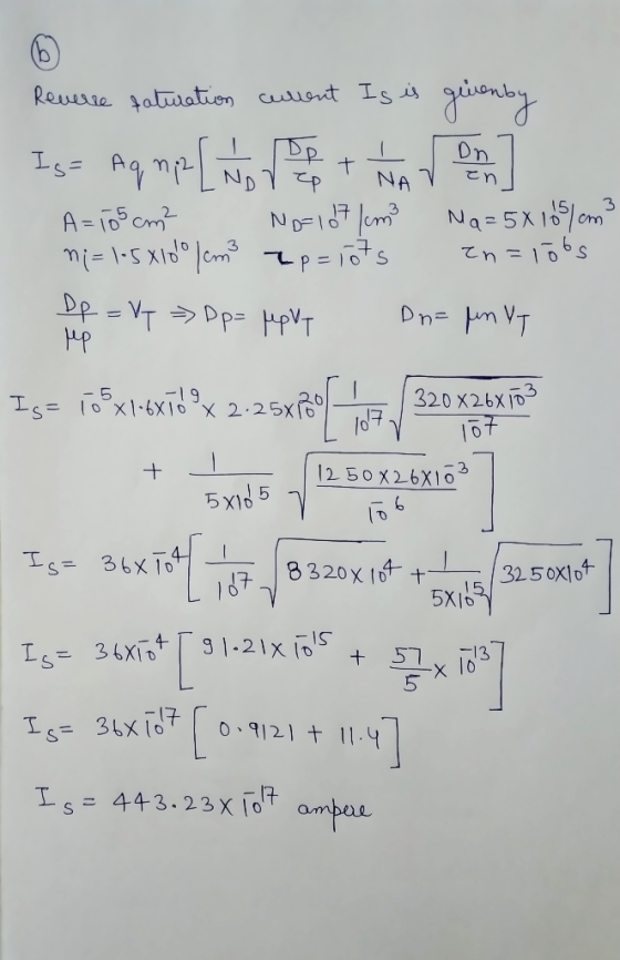
 A silicon pn junction at T = 300 K has the following parameters: Na-5 1016 cm-?, N,-1 1016 cm-3, D.-25 cm3/s, D.-10 cm2/s, ?,0-5 x 10⁻⁷ s, and To 1 X 10⁻⁷ s. The cross-sectional area is A 10-3 cm2 and the forward- bias voltage is V,-0.625 V. Calculate the (a) minority electron diffusion cur- rent at the space charge edge, (b) minority hole diffusion current at the space charge edge, and (c) total current in the pn junction diode.
A silicon PN junction diode is constructed using N-type silicon in which the Fermi level is...
 A silicon PN junction diode is constructed using N-type silicon in which the Fermi level is 100 meV below the conduction band edge and P-type silicon in which the Fermi level is 120 meV above the valence band edge a) What are the majority and minority carrier concentrations on each side of the junction under thermal equilibrium? b) What is the value of the built-in voltage? c) Determine the width of the depletion region on both sides of the junction...
Q3 Consider a GaAs pn junction with doping concentrations Na5 x 106 cm-3 and N1016 cm-3....
 Q3 Consider a GaAs pn junction with doping concentrations Na5 x 106 cm-3 and N1016 cm-3. The junction cross-sectional area is A 103 cm2 and the applied forward-bias voltage is Va 1.10 V. Calculate the (a) minority electron diffusion cur rent at the edge of the space charge region, (b) minority hole diffusion current at the edge of the space charge region, and (c) total current in the pn junction diode.
Design an ideal abrupt silicon PN-junction at 300 K such that the donor impurity concentration in...
 XXX is 467
Design an ideal abrupt silicon PN-junction at 300 K such that the donor impurity concentration in the n-side N, = 5x1015 cm3 and the acceptor impurity concentration in the p-side N, = XXX × 1015/cm3 Assume that the diode area A-2x10⁻³ cm2 and 100cm work Note that the values obtained in the calculations may not be realistic as the Matric # varies greatly. The assignment is only to test your understanding, and must be handwritten Determine the...
XXX is 467
Design an ideal abrupt silicon PN-junction at 300 K such that the donor impurity concentration in the n-side N, = 5x1015 cm3 and the acceptor impurity concentration in the p-side N, = XXX × 1015/cm3 Assume that the diode area A-2x10⁻³ cm2 and 100cm work Note that the values obtained in the calculations may not be realistic as the Matric # varies greatly. The assignment is only to test your understanding, and must be handwritten Determine the...
Consider a silicon pn step junction diode with NA-1x1018 cm3 and No 1x1017cm-3, maintained at T...
 Consider a silicon pn step junction diode with NA-1x1018 cm3 and No 1x1017cm-3, maintained at T 300K. The minority carrier lifetimes in the p-side and n-side are τη-10-8 s and Tp-10-7 s, respectively. a) Calculate the minority carrier densities at the edges of the depletion region when the applied voltage (VA) is 0.6 V. of the junction, for the applied bias voltage of part (a) densities are equal in magnitude, for the applied voltage of part (a). b) Sketch the...
3.13 Si pn junction Consider a long pn junction diode with an acceptor doping Naof 1018...
 3.13 Si pn junction Consider a long pn junction diode with an acceptor doping Naof 1018 cm-3 on the p-side and donor concentration of Nj on the n-side. The diode is forward biased and has a voltage of 0.6 V across it. The diode cross-sectional area is 1 mm2. The minority carrier recombination time, T, depends on the total dopant concentration, Ndopant (cm), through the following approximate empirical relation (5x 10⁻⁷)/(1 + 2 10-17N1°pan.) where T is in seconds. (a)...
consider a silicon pn junction diode at 300 K with nd= na = 10^16 cm-3, u_n 1350 cm^2/v-s, u_p 480 cm^2/v-s, and t_no = t_po= 5×10^-7 s. consider two bias conditions: i) a reverse bias of 1.0 v ii) a...
consider a silicon pn junction diode at 300 K with nd= na = 10^16 cm-3, u_n 1350 cm^2/v-s, u_p 480 cm^2/v-s, and t_no = t_po= 5×10^-7 s. consider two bias conditions: i) a reverse bias of 1.0 v ii) a forward bias of 0.2 v a) for each bus condition, roughly sketch the band gap diagram - accurately label the energy gap in eV - indicate the difference between E_f on the two sides id the junction and label its...
 Q2 (24%) A Si PN junction is operating at 300K. The device parameters are as follows: Na 5X10¹⁶ /cm3 D2-10cm2ls Na 1X10¹⁶/cm3 D-25 cm2Is Tpo=T10= 5X1078 a. Calculate Vhi . b. Calculate xn and xp c. Plot the electric field strength across the entire pn junction and calculate the peak electric field in the space charge region d. If a forward bias voltage of 0.7V is applied, find the forward current density e. Draw the energy band diagram for the...
 Problem 4: Narrow-Base Diode Consider an ideal pn* step-junction Si diode maintained at 300K with cross-sectional area A = 104cm2. The doping concentration on the p-type side is Na= 1017 cm3 (uncompensated). (The n-type side is degenerately doped.) The electron recombination lifetime in the p-type region is tn = 10-6 s. The width of the quasi-neutral p-type region is 1 um, for VA=0 V. a Is this a narrow-base diode? Justify your answer. b) Calculate the diode saturation current Io....
 A pn iunction diode has the following parameters, Na-2x10^17 Dp 10.36 Tp - 5x10-'s Area is 1mm 2 Nc-1x10 16 Dn-18.13 Tn-5x10-s Length of diode is 100 mm At equilibrium, what is the width of the depletion region, the built in potential, the electric field across the depletion region and the capacitance of the depletion region a. b. Can you tell from the doping levels which region the depletion regioin c. Find the Fermi level in both regions and the...
 A silicon pn junction at T = 300 K has the following parameters: Na-5 1016 cm-?, N,-1 1016 cm-3, D.-25 cm3/s, D.-10 cm2/s, ?,0-5 x 10⁻⁷ s, and To 1 X 10⁻⁷ s. The cross-sectional area is A 10-3 cm2 and the forward- bias voltage is V,-0.625 V. Calculate the (a) minority electron diffusion cur- rent at the space charge edge, (b) minority hole diffusion current at the space charge edge, and (c) total current in the pn junction diode.
 A silicon PN junction diode is constructed using N-type silicon in which the Fermi level is 100 meV below the conduction band edge and P-type silicon in which the Fermi level is 120 meV above the valence band edge a) What are the majority and minority carrier concentrations on each side of the junction under thermal equilibrium? b) What is the value of the built-in voltage? c) Determine the width of the depletion region on both sides of the junction...
 Q3 Consider a GaAs pn junction with doping concentrations Na5 x 106 cm-3 and N1016 cm-3. The junction cross-sectional area is A 103 cm2 and the applied forward-bias voltage is Va 1.10 V. Calculate the (a) minority electron diffusion cur rent at the edge of the space charge region, (b) minority hole diffusion current at the edge of the space charge region, and (c) total current in the pn junction diode.
 XXX is 467
Design an ideal abrupt silicon PN-junction at 300 K such that the donor impurity concentration in the n-side N, = 5x1015 cm3 and the acceptor impurity concentration in the p-side N, = XXX × 1015/cm3 Assume that the diode area A-2x10⁻³ cm2 and 100cm work Note that the values obtained in the calculations may not be realistic as the Matric # varies greatly. The assignment is only to test your understanding, and must be handwritten Determine the...
XXX is 467
Design an ideal abrupt silicon PN-junction at 300 K such that the donor impurity concentration in the n-side N, = 5x1015 cm3 and the acceptor impurity concentration in the p-side N, = XXX × 1015/cm3 Assume that the diode area A-2x10⁻³ cm2 and 100cm work Note that the values obtained in the calculations may not be realistic as the Matric # varies greatly. The assignment is only to test your understanding, and must be handwritten Determine the...
 Consider a silicon pn step junction diode with NA-1x1018 cm3 and No 1x1017cm-3, maintained at T 300K. The minority carrier lifetimes in the p-side and n-side are τη-10-8 s and Tp-10-7 s, respectively. a) Calculate the minority carrier densities at the edges of the depletion region when the applied voltage (VA) is 0.6 V. of the junction, for the applied bias voltage of part (a) densities are equal in magnitude, for the applied voltage of part (a). b) Sketch the...
 3.13 Si pn junction Consider a long pn junction diode with an acceptor doping Naof 1018 cm-3 on the p-side and donor concentration of Nj on the n-side. The diode is forward biased and has a voltage of 0.6 V across it. The diode cross-sectional area is 1 mm2. The minority carrier recombination time, T, depends on the total dopant concentration, Ndopant (cm), through the following approximate empirical relation (5x 10⁻⁷)/(1 + 2 10-17N1°pan.) where T is in seconds. (a)...
Most questions answered within 3 hours.
-
(a) A piston at 6.1 atm contains a gas that occupies a volume of
3.5 L....
asked 1 hour ago -
Please answer true or false. Words
cannot be changed or added in to make it true...
asked 1 hour ago -
An empty test tube weighs 15.923 grams. Then,
MgCl2•6H2O is added into the test tube. After...
asked 1 hour ago -
Assume memory access is 10 units of time and disk access is
10000 units of time....
asked 1 hour ago -
1. Are all good samples random?
2. Magazines often report surveys giving statistics such as “63%...
asked 1 hour ago -
Under all the various types of market structures, firms
must eventually earn some economic profits for...
asked 1 hour ago -
Consider the following fitness regime for a single locus trait
with two co-dominant alleles: w11 =...
asked 1 hour ago -
A large cable company reports the following.
80% of its customers subscribe to its cable TV...
asked 1 hour ago -
Please answer the question in brief.
Discuss the role of ERP in organizations. Are ERP tools...
asked 1 hour ago -
Discuss the pros and cons of collaborative software such
as SameTime. Does it increase productivity? What...
asked 1 hour ago -
Buying your in-laws a gift because it’s expected is
due to the ____________ motive of gift-giving....
asked 1 hour ago -
Calculate the expected value, the variance, and the standard
deviation of the given random variable X....
asked 2 hours ago