
Homework Answers
![Problem 3 Given circuit Plan for de operating point (All Capacitors cae open] . vt. uv VERS Skry Rc = UK - 6V apply kul to en](http://img.homeworklib.com/questions/27bd70e0-b6f3-11ea-a54b-8b96472e4040.png?x-oss-process=image/resize,w_560)
Add Answer to:
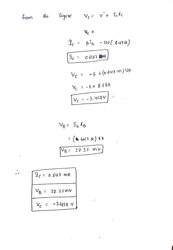
Problem 3. In the circuit below, assuming has B = 100 and VEB=0.7V, find Ic, VB...
Problem 2 (15 points) In the circuit below, the transistor has B=50 and VEB = 0.7V....
 Problem 2 (15 points) In the circuit below, the transistor has B=50 and VEB = 0.7V. Find the values of VB, VE, and Vc, and verify that the transistor is operating in the active mode. What is the largest value that Rc can have while the transistor remains in the active mode? +3V SR 3222 Vio R: 20 ks OV -
2) Consider the circuit below. Assume B=49 A/A, VBe=0.7V, VCEsat=0.2V. If the Collector current is Ic...
 2) Consider the circuit below. Assume B=49 A/A, VBe=0.7V, VCEsat=0.2V. If the Collector current is Ic = 9.8 mA, Find Vc, VE, VB and VBB; as well as the currents IE and IB. Hint: VBB>0. Verify your assumption. 15V V BB ic 3 Rc CS 30622 AVC RB 10k 2 B E → VE ięRE ES 33012
a) Find the operating point (Ic and Vce) of the circuit shown in below. b) The...
 a) Find the operating point (Ic and Vce) of the circuit shown in below. b) The BJT is biased at Ic = 1.5mA.Find the value of the VEE when all other parameters remain same I Vcc=5V + R 5k RA C- 260k PE=200 UT V26mV VB=0.7V -Ve=-2V
(20 pts) The BJT in the circuit below has the following specifications: • in active mode...
 (20 pts) The BJT in the circuit below has the following specifications: • in active mode ß = 50, VBE = 0.76 V, and • in saturation VCEsat = 0.2 V. Find VE, VB and Vc and determine the mode of operation (active, saturation, cut-off). Given values are: /= 1 mA, Rg=200 kN and Re =4 k12. I Vc RB VB. VEم RE
Professor: Farid Tranjan +5 V Name:- 0.7V (50 points). Q1: For the BJT circuit, B- 100...
 Professor: Farid Tranjan +5 V Name:- 0.7V (50 points). Q1: For the BJT circuit, B- 100 and VE Find Re and Rg such that Ico =0.25 mA and VCEO b. Find the DCLL = 3 V a. R: 50 k0 So.1 kn Find the ACLL c. to find the maximum symmetrical swing in Vo Vo Draw the small-signal t-model and find the gain Ay d. Plot DCLLUACLL e. Vi
Professor: Farid Tranjan +5 V Name:- 0.7V (50 points). Q1: For...
Professor: Farid Tranjan +5 V Name:- 0.7V (50 points). Q1: For the BJT circuit, B- 100 and VE Find Re and Rg such that Ico =0.25 mA and VCEO b. Find the DCLL = 3 V a. R: 50 k0 So.1 kn Find the ACLL c. to find the maximum symmetrical swing in Vo Vo Draw the small-signal t-model and find the gain Ay d. Plot DCLLUACLL e. Vi
Professor: Farid Tranjan +5 V Name:- 0.7V (50 points). Q1: For...
BJT DC Operating Points and AC small signal parameters. ) For the BJT circuit below, calculate...
 BJT DC Operating Points and AC small signal parameters. ) For the BJT circuit below, calculate the DC values for Vc, VB. VE, c, IB, and IE. Compute the AC small signal parameters gm, Tz, Te. Assume the transistor p-150, VBE 0.7V, and V 25.9mV 10V Vc Ic VB Is VeE R82 100kΩ RE1 100 RE22k0
The transistor in the circuit below has ?-100 and Vci(sat) OV. You may use the constant...
 The transistor in the circuit below has ?-100 and Vci(sat) OV. You may use the constant voltage model with VE 0.7V if the base emitter junction is forward biased. A variable DC source is attached to input VIN. Find the operating mode (cutoff, active, or saturation), the collector node voltage VC, and the collector current IC for each of the following cases: (a) VIN 0V (b) VIN = 1.2V (c) VIN 6.0v (d) VIN 12.0V 1 K IC VC 10K...
Problem 4 (20 %) For the circuit shown in Figure 4 determine IB, IC, and VC....
 Problem 4 (20 %) For the circuit shown in Figure 4 determine IB,
IC, and VC. Data VCC=9 V VBB=4 V R2= 165 k R1= 2.5 k Transistor
Assume VBE ≈ 0.7 V and =150
Derive all the results. Give the answers with the preestablished
prefix.
FAVOR DIBUJAR LOS CIRCUITOS
Problem 4 (206) For the circuit shown in Figure 4 determine IB, I, and Vc. Data Ve=9 V V=4V R = 165 kg R=2.5k_2 Transistor Assume VE 0.7 V and...
Problem 4 (20 %) For the circuit shown in Figure 4 determine IB,
IC, and VC. Data VCC=9 V VBB=4 V R2= 165 k R1= 2.5 k Transistor
Assume VBE ≈ 0.7 V and =150
Derive all the results. Give the answers with the preestablished
prefix.
FAVOR DIBUJAR LOS CIRCUITOS
Problem 4 (206) For the circuit shown in Figure 4 determine IB, I, and Vc. Data Ve=9 V V=4V R = 165 kg R=2.5k_2 Transistor Assume VE 0.7 V and...
(2+5 pts) Consider the bias circuit below for a transistor amplifier designed for active region operation....
 (2+5 pts) Consider the bias circuit below for a transistor amplifier designed for active region operation. The desired bias point parameters are lg = 3 mA and Ic = 2.97 mA. Assume VBE- 0.7 V and VT=25 mV. Determine the emitter voltage VE . Choose the best answer. VCC +15 V Vc RBB VB LVE V BB RE 500 S2 1.49 V O2v 01.5V O 0.7V
RE 3K30 V_B Dar v.ce vor RC ROOLIVC B = 100 and VBE = -0.7V Fig....
 RE 3K30 V_B Dar v.ce vor RC ROOLIVC B = 100 and VBE = -0.7V Fig. 2 1. Calculate: VB.Ve V, and Vce. 2. Calculate:IB., and Ic. 3. Using the same circuit and assuming active mode operation, find the resistor values (R1, R2, Re and Rc), to bias the transistor at the Q-point: Vce = -8 V and Ic = 8 mA. Use the following parameters: Vcc = 20 V,ß = 200,Ve = 16 V, RTH = 0.1BRg.
 Problem 2 (15 points) In the circuit below, the transistor has B=50 and VEB = 0.7V. Find the values of VB, VE, and Vc, and verify that the transistor is operating in the active mode. What is the largest value that Rc can have while the transistor remains in the active mode? +3V SR 3222 Vio R: 20 ks OV -
 2) Consider the circuit below. Assume B=49 A/A, VBe=0.7V, VCEsat=0.2V. If the Collector current is Ic = 9.8 mA, Find Vc, VE, VB and VBB; as well as the currents IE and IB. Hint: VBB>0. Verify your assumption. 15V V BB ic 3 Rc CS 30622 AVC RB 10k 2 B E → VE ięRE ES 33012
 a) Find the operating point (Ic and Vce) of the circuit shown in below. b) The BJT is biased at Ic = 1.5mA.Find the value of the VEE when all other parameters remain same I Vcc=5V + R 5k RA C- 260k PE=200 UT V26mV VB=0.7V -Ve=-2V
 (20 pts) The BJT in the circuit below has the following specifications: • in active mode ß = 50, VBE = 0.76 V, and • in saturation VCEsat = 0.2 V. Find VE, VB and Vc and determine the mode of operation (active, saturation, cut-off). Given values are: /= 1 mA, Rg=200 kN and Re =4 k12. I Vc RB VB. VEم RE
 Professor: Farid Tranjan +5 V Name:- 0.7V (50 points). Q1: For the BJT circuit, B- 100 and VE Find Re and Rg such that Ico =0.25 mA and VCEO b. Find the DCLL = 3 V a. R: 50 k0 So.1 kn Find the ACLL c. to find the maximum symmetrical swing in Vo Vo Draw the small-signal t-model and find the gain Ay d. Plot DCLLUACLL e. Vi
Professor: Farid Tranjan +5 V Name:- 0.7V (50 points). Q1: For...
Professor: Farid Tranjan +5 V Name:- 0.7V (50 points). Q1: For the BJT circuit, B- 100 and VE Find Re and Rg such that Ico =0.25 mA and VCEO b. Find the DCLL = 3 V a. R: 50 k0 So.1 kn Find the ACLL c. to find the maximum symmetrical swing in Vo Vo Draw the small-signal t-model and find the gain Ay d. Plot DCLLUACLL e. Vi
Professor: Farid Tranjan +5 V Name:- 0.7V (50 points). Q1: For...
 BJT DC Operating Points and AC small signal parameters. ) For the BJT circuit below, calculate the DC values for Vc, VB. VE, c, IB, and IE. Compute the AC small signal parameters gm, Tz, Te. Assume the transistor p-150, VBE 0.7V, and V 25.9mV 10V Vc Ic VB Is VeE R82 100kΩ RE1 100 RE22k0
 The transistor in the circuit below has ?-100 and Vci(sat) OV. You may use the constant voltage model with VE 0.7V if the base emitter junction is forward biased. A variable DC source is attached to input VIN. Find the operating mode (cutoff, active, or saturation), the collector node voltage VC, and the collector current IC for each of the following cases: (a) VIN 0V (b) VIN = 1.2V (c) VIN 6.0v (d) VIN 12.0V 1 K IC VC 10K...
 Problem 4 (20 %) For the circuit shown in Figure 4 determine IB,
IC, and VC. Data VCC=9 V VBB=4 V R2= 165 k R1= 2.5 k Transistor
Assume VBE ≈ 0.7 V and =150
Derive all the results. Give the answers with the preestablished
prefix.
FAVOR DIBUJAR LOS CIRCUITOS
Problem 4 (206) For the circuit shown in Figure 4 determine IB, I, and Vc. Data Ve=9 V V=4V R = 165 kg R=2.5k_2 Transistor Assume VE 0.7 V and...
Problem 4 (20 %) For the circuit shown in Figure 4 determine IB,
IC, and VC. Data VCC=9 V VBB=4 V R2= 165 k R1= 2.5 k Transistor
Assume VBE ≈ 0.7 V and =150
Derive all the results. Give the answers with the preestablished
prefix.
FAVOR DIBUJAR LOS CIRCUITOS
Problem 4 (206) For the circuit shown in Figure 4 determine IB, I, and Vc. Data Ve=9 V V=4V R = 165 kg R=2.5k_2 Transistor Assume VE 0.7 V and...
 (2+5 pts) Consider the bias circuit below for a transistor amplifier designed for active region operation. The desired bias point parameters are lg = 3 mA and Ic = 2.97 mA. Assume VBE- 0.7 V and VT=25 mV. Determine the emitter voltage VE . Choose the best answer. VCC +15 V Vc RBB VB LVE V BB RE 500 S2 1.49 V O2v 01.5V O 0.7V
 RE 3K30 V_B Dar v.ce vor RC ROOLIVC B = 100 and VBE = -0.7V Fig. 2 1. Calculate: VB.Ve V, and Vce. 2. Calculate:IB., and Ic. 3. Using the same circuit and assuming active mode operation, find the resistor values (R1, R2, Re and Rc), to bias the transistor at the Q-point: Vce = -8 V and Ic = 8 mA. Use the following parameters: Vcc = 20 V,ß = 200,Ve = 16 V, RTH = 0.1BRg.
Most questions answered within 3 hours.
-
Which of the following pairs of ions have the same electron
configuration?
I: Br− and Se2−...
asked 2 hours ago -
The Foremost Composite Materials Company is planning a two-day
sales conference for October 19-20. The conference...
asked 2 hours ago -
3) Illustrate the observed pattern of relatedness of organisms
versus adaptations to specific conditions. This means...
asked 2 hours ago -
In winter a lake has a 0.35 m thick ice layer over 1.10 m of
water....
asked 3 hours ago -
Assuming the following has been encrypted with a Vigenere cipher
below, use the method(s) and assumptions...
asked 4 hours ago -
How would I use switch statements to write a program that will
take an input of...
asked 3 hours ago -
Imagine a reaction in which methane gas combusts at a constant
pressure of 1 atm and...
asked 4 hours ago -
Two parallel wires (each 12 m in length) are separated by a
distance of 0.065 m...
asked 4 hours ago -
Suppose there were three masses at the corner of uniform
equilateral triangle. The masses are m1...
asked 4 hours ago -
Situation: A building that is 618 m above the ground floor. How
many times would a...
asked 4 hours ago -
help me and discuss one successful and one
unsuccessful international company/busines in Indonesia.whyit
succeed and why...
asked 4 hours ago -
I- Choose the best answer
Which of the following statements about the structure and
packaging of...
asked 4 hours ago