
Homework Answers
According to the question there are four inputs (let say W, X, Y, Z) and 7 outputs (A, B, C, D, E, F, G), these 7 outputs are the segments of the decoder, the arrangement of these 7 segments are as follows:-

The truth table of BCD-to seven segment decoder is as follows:-
| W | X | Y | Z | A | B | C | D | E | F | G |
|---|---|---|---|---|---|---|---|---|---|---|
| 0 | 0 | 0 | 0 | 1 | 1 | 1 | 1 | 1 | 1 | 0 |
| 0 | 0 | 0 | 1 | 1 | 1 | 0 | 0 | 0 | 0 | 0 |
| 0 | 0 | 1 | 0 | 1 | 0 | 1 | 1 | 1 | 0 | 1 |
| 0 | 0 | 1 | 1 | 1 | 1 | 1 | 1 | 0 | 0 | 1 |
| 0 | 1 | 0 | 0 | 1 | 1 | 0 | 0 | 0 | 1 | 1 |
| 0 | 1 | 0 | 1 | 0 | 1 | 1 | 1 | 0 | 1 | 1 |
| 0 | 1 | 1 | 0 | 0 | 1 | 1 | 1 | 1 | 1 | 1 |
| 0 | 1 | 1 | 1 | 1 | 1 | 1 | 0 | 0 | 0 | 0 |
| 1 | 0 | 0 | 0 | 1 | 1 | 1 | 1 | 1 | 1 | 1 |
| 1 | 0 | 0 | 1 | 1 | 1 | 1 | 1 | 0 | 1 | 1 |
| 1 | 0 | 1 | 0 | X | X | X | X | X | X | X |
| 1 | 0 | 1 | 1 | X | X | X | X | X | X | X |
| 1 | 1 | 0 | 0 | X | X | X | X | X | X | X |
| 1 | 1 | 0 | 1 | X | X | X | X | X | X | X |
| 1 | 1 | 1 | 0 | X | X | X | X | X | X | X |
| 1 | 1 | 1 | 1 | X | X | X | X | X | X | X |
Since BCD values are only valid from 0 to 9 therefore for the rest combinations (10-15) the value of 7 segment decoder will be blank, since blank do not have any fixed value therefore we used (don't care).
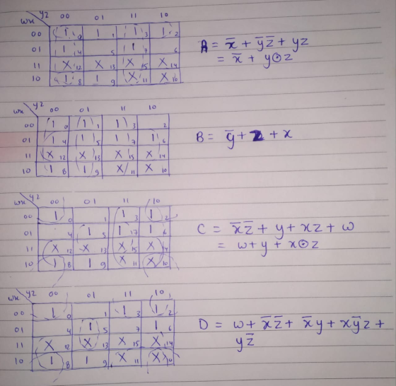
Using above truth table the equations for each output segment using K-map is derived as follows:-

Using above equations the circuit diagram of the BCD- seven segment decoder is as follows:-
 From the above equations the number of input gates required are as
follows:-
From the above equations the number of input gates required are as
follows:-
| Segment | AND gate | OR gate |
|---|---|---|
| A | 2 | 2 |
| B | 0 | 2 |
| C | 2 | 3 |
| D | 5 | 4 |
| E | 2 | 1 |
| F | 3 | 3 |
| G | 3 | 3 |
These are the maximum number of input gates (total 17 AND, 18 OR) that can be used in designing the above circuit, but this can be minimized by using the same circuit for common product terms.
Add Answer to:
could use some help with this. please show work so that i can
understand how its...
after completing the truth table, write equations for each output segment. ( through Sa-Sg so 7...
 after completing the truth table, write equations for each output
segment. ( through Sa-Sg so 7 equations) using k-maps
next translate your equations into logic gates using
only ONE design for all the equations.
7-segment 4, display7 decoder S Figure 3.7-segment display decoder To design your seven-segment display decoder, you will first write the truth table specifying the output values for each input combination. We have started the truth table for you in Table 1. For example, when the input...
after completing the truth table, write equations for each output
segment. ( through Sa-Sg so 7 equations) using k-maps
next translate your equations into logic gates using
only ONE design for all the equations.
7-segment 4, display7 decoder S Figure 3.7-segment display decoder To design your seven-segment display decoder, you will first write the truth table specifying the output values for each input combination. We have started the truth table for you in Table 1. For example, when the input...
A combinational circuit is used to control a seven-segment display of decimal digits, as shown in...
 A combinational circuit is used to control a seven-segment display of decimal digits, as shown in Figure 11.35. The circuit has four inputs, which provide the four-bit code used in packed decimal representation (0_10=0000, ..., 9_10=1001). The seven outputs define which segments will be activated to display a given decimal digit. Note that some combinations of inputs and outputs are not needed. Develop a truth table for this circuit. Express the truth table in SOP form. Express the truth table...
The seven-segment indicator (shown in the figure) can be used to display any of the decimal digits 0 through 9. For example "1" is displayed by lighting segment 2 and 3 and "8" by...
 The seven-segment indicator (shown in the figure) can be used to display any of the decimal digits 0 through 9. For example "1" is displayed by lighting segment 2 and 3 and "8" by lighting all seven segments. A segment is lighted when logic 1 is applied to the corresponding input on the display module. Circuit to be aputs From Switche l p Designed Design an excess-3 code convertor to derive a seven segment indicator. The four inputs to the...
2. The decimal digits 0 to 9 are represented by four logic signals using the 7321 weighted BCD code. Only the code...
 2. The decimal digits 0 to 9 are represented by four logic signals using the 7321 weighted BCD code. Only the code 0011 is used to represent the digit 3. In addition the code 1100 is used to represent the character E. Codes that do not represent either a decimal digit (including 0100), or the character E never occur. The logic signals are inputs to a decoder circuit whose outputs provide drive signals for a seven segment display system shown...
Design an excess-3 code converter to drive a seven-segment indicator. The four inputs to the conv...
 can someone help me solve this please
Design an excess-3 code converter to drive a seven-segment indicator. The four inputs to the converter circuit represent an excess-3 coded decimal digit. Assume that only input combinations representing the digits 0 through 9 can occur as inputs, so that the six unused combinations are don't-cares. Implement the circuits using Decoder(s) (active low) and any necessary external gates and a separate solution using Multiplexer(S) and any necessary external gates Please specify the integrated...
can someone help me solve this please
Design an excess-3 code converter to drive a seven-segment indicator. The four inputs to the converter circuit represent an excess-3 coded decimal digit. Assume that only input combinations representing the digits 0 through 9 can occur as inputs, so that the six unused combinations are don't-cares. Implement the circuits using Decoder(s) (active low) and any necessary external gates and a separate solution using Multiplexer(S) and any necessary external gates Please specify the integrated...
ECE 1552- Summer 2019 Homework 2: Solve all questions. HW is to be turned in as a PDF or word document on canvas. Show...
 ECE 1552- Summer 2019 Homework 2: Solve all questions. HW is to be turned in as a PDF or word document on canvas. Show all working. Answers provided should be typed or written CLEARLY 1: Find a function to detect an error in the representation of a decimal digit in BCD. In other words, write an equation with value 1 when the inputs are any one of the six unused bit combinations in the BCD code, and value 0 otherwise...
**ONLY C&D PLEASE!** (100 points) You are asked to design a "HELLO" circuit in this question....
 **ONLY C&D PLEASE!**
(100 points) You are asked to design a "HELLO" circuit in this question. The inputs of the circuit are three bits x, y and z. The outputs are seven bits a, b, c, d, e, f and g controlling a 7-segment display (see Fig. 2.63(a)). For the 7-segment display, a segment is turned on when the corresponding control signal is 1. The "HELLO" circuit outputs the control signals to display the letter "H", "E", "L", "L", "O"...
**ONLY C&D PLEASE!**
(100 points) You are asked to design a "HELLO" circuit in this question. The inputs of the circuit are three bits x, y and z. The outputs are seven bits a, b, c, d, e, f and g controlling a 7-segment display (see Fig. 2.63(a)). For the 7-segment display, a segment is turned on when the corresponding control signal is 1. The "HELLO" circuit outputs the control signals to display the letter "H", "E", "L", "L", "O"...
Design the logic circuit to display a 3 bit octal numbers from 0 to 7 on...
 Design the logic circuit to display a 3 bit octal numbers from 0 to 7 on a seven segment display shown below (for number 1 use segments b and c; for 6 include segment (a) Write the Truth Table with A, B. C representing the input bits (A is the MSB) and a, b, c, d, e, f and g representing the outputs to the seven segments. (b) Implement the circuit using a Programmable Logic Array (use simplified notation to...
NOTE: PLEASE USE FEWEST NUMBER OF COMPONENTS POSSIBLE FOR EACH IMPLEMENTATION? 5.(20 PTS) A combinational circuit...
 NOTE: PLEASE USE FEWEST NUMBER OF COMPONENTS POSSIBLE FOR EACH
IMPLEMENTATION?
5.(20 PTS) A combinational circuit converts an Excess-3 input (ABCD) into a Hexidecimal output displayed on a seven segment display (a,b,c,d,e,f,g). All invalid combinations (negative numbers) are don't cares. . E Represent 6 as and 9 as I - algla di 16 Represent hexadecimal letters in capital letters if possible. Show how you represent the letters with seven segment indicators as above for 6 and 9. Show how you...
NOTE: PLEASE USE FEWEST NUMBER OF COMPONENTS POSSIBLE FOR EACH
IMPLEMENTATION?
5.(20 PTS) A combinational circuit converts an Excess-3 input (ABCD) into a Hexidecimal output displayed on a seven segment display (a,b,c,d,e,f,g). All invalid combinations (negative numbers) are don't cares. . E Represent 6 as and 9 as I - algla di 16 Represent hexadecimal letters in capital letters if possible. Show how you represent the letters with seven segment indicators as above for 6 and 9. Show how you...
Building and testing basic combinational circuits using Verilog HDL Description: Build and test t...
Building and testing basic combinational circuits using Verilog HDL Description: Build and test the following circuits using gate-level modeling in Verilog HDL. 1. 3-input majority function. 2. Conditional inverter (see the table below: x - control input, y - data input). Do NOT use XOR gates for the implementation. x y Output 0 y 1 y' 3. Two-input multiplexer (see the table below: x,y - data inputs, z - control input). z Output 0 x 1 y 4. 1-bit half...
 after completing the truth table, write equations for each output
segment. ( through Sa-Sg so 7 equations) using k-maps
next translate your equations into logic gates using
only ONE design for all the equations.
7-segment 4, display7 decoder S Figure 3.7-segment display decoder To design your seven-segment display decoder, you will first write the truth table specifying the output values for each input combination. We have started the truth table for you in Table 1. For example, when the input...
after completing the truth table, write equations for each output
segment. ( through Sa-Sg so 7 equations) using k-maps
next translate your equations into logic gates using
only ONE design for all the equations.
7-segment 4, display7 decoder S Figure 3.7-segment display decoder To design your seven-segment display decoder, you will first write the truth table specifying the output values for each input combination. We have started the truth table for you in Table 1. For example, when the input...
 A combinational circuit is used to control a seven-segment display of decimal digits, as shown in Figure 11.35. The circuit has four inputs, which provide the four-bit code used in packed decimal representation (0_10=0000, ..., 9_10=1001). The seven outputs define which segments will be activated to display a given decimal digit. Note that some combinations of inputs and outputs are not needed. Develop a truth table for this circuit. Express the truth table in SOP form. Express the truth table...
 The seven-segment indicator (shown in the figure) can be used to display any of the decimal digits 0 through 9. For example "1" is displayed by lighting segment 2 and 3 and "8" by lighting all seven segments. A segment is lighted when logic 1 is applied to the corresponding input on the display module. Circuit to be aputs From Switche l p Designed Design an excess-3 code convertor to derive a seven segment indicator. The four inputs to the...
 2. The decimal digits 0 to 9 are represented by four logic signals using the 7321 weighted BCD code. Only the code 0011 is used to represent the digit 3. In addition the code 1100 is used to represent the character E. Codes that do not represent either a decimal digit (including 0100), or the character E never occur. The logic signals are inputs to a decoder circuit whose outputs provide drive signals for a seven segment display system shown...
 can someone help me solve this please
Design an excess-3 code converter to drive a seven-segment indicator. The four inputs to the converter circuit represent an excess-3 coded decimal digit. Assume that only input combinations representing the digits 0 through 9 can occur as inputs, so that the six unused combinations are don't-cares. Implement the circuits using Decoder(s) (active low) and any necessary external gates and a separate solution using Multiplexer(S) and any necessary external gates Please specify the integrated...
can someone help me solve this please
Design an excess-3 code converter to drive a seven-segment indicator. The four inputs to the converter circuit represent an excess-3 coded decimal digit. Assume that only input combinations representing the digits 0 through 9 can occur as inputs, so that the six unused combinations are don't-cares. Implement the circuits using Decoder(s) (active low) and any necessary external gates and a separate solution using Multiplexer(S) and any necessary external gates Please specify the integrated...
 ECE 1552- Summer 2019 Homework 2: Solve all questions. HW is to be turned in as a PDF or word document on canvas. Show all working. Answers provided should be typed or written CLEARLY 1: Find a function to detect an error in the representation of a decimal digit in BCD. In other words, write an equation with value 1 when the inputs are any one of the six unused bit combinations in the BCD code, and value 0 otherwise...
 **ONLY C&D PLEASE!**
(100 points) You are asked to design a "HELLO" circuit in this question. The inputs of the circuit are three bits x, y and z. The outputs are seven bits a, b, c, d, e, f and g controlling a 7-segment display (see Fig. 2.63(a)). For the 7-segment display, a segment is turned on when the corresponding control signal is 1. The "HELLO" circuit outputs the control signals to display the letter "H", "E", "L", "L", "O"...
**ONLY C&D PLEASE!**
(100 points) You are asked to design a "HELLO" circuit in this question. The inputs of the circuit are three bits x, y and z. The outputs are seven bits a, b, c, d, e, f and g controlling a 7-segment display (see Fig. 2.63(a)). For the 7-segment display, a segment is turned on when the corresponding control signal is 1. The "HELLO" circuit outputs the control signals to display the letter "H", "E", "L", "L", "O"...
 Design the logic circuit to display a 3 bit octal numbers from 0 to 7 on a seven segment display shown below (for number 1 use segments b and c; for 6 include segment (a) Write the Truth Table with A, B. C representing the input bits (A is the MSB) and a, b, c, d, e, f and g representing the outputs to the seven segments. (b) Implement the circuit using a Programmable Logic Array (use simplified notation to...
 NOTE: PLEASE USE FEWEST NUMBER OF COMPONENTS POSSIBLE FOR EACH
IMPLEMENTATION?
5.(20 PTS) A combinational circuit converts an Excess-3 input (ABCD) into a Hexidecimal output displayed on a seven segment display (a,b,c,d,e,f,g). All invalid combinations (negative numbers) are don't cares. . E Represent 6 as and 9 as I - algla di 16 Represent hexadecimal letters in capital letters if possible. Show how you represent the letters with seven segment indicators as above for 6 and 9. Show how you...
NOTE: PLEASE USE FEWEST NUMBER OF COMPONENTS POSSIBLE FOR EACH
IMPLEMENTATION?
5.(20 PTS) A combinational circuit converts an Excess-3 input (ABCD) into a Hexidecimal output displayed on a seven segment display (a,b,c,d,e,f,g). All invalid combinations (negative numbers) are don't cares. . E Represent 6 as and 9 as I - algla di 16 Represent hexadecimal letters in capital letters if possible. Show how you represent the letters with seven segment indicators as above for 6 and 9. Show how you...
Most questions answered within 3 hours.
-
SQL help:
Design a database diagram for a database that stores information
about the Downloads that...
asked 23 minutes ago -
In 1970s and 1980s, molecular biologists discovered that the
hormone testosterone, binds a receptor protein that...
asked 2 hours ago -
january 1 2010 road catering service purchase a piece of
equipment for 58000 which is expected...
asked 2 hours ago -
Explain Mertons concept of anomie is and what the
modes of adaptation to it are?
asked 3 hours ago -
Jamie is doing a survey at her school about whether the students
feel the cafeteria food...
asked 5 hours ago -
How many liters of 0.669 M KOH will be needed to raise the pH of
0.339...
asked 7 hours ago -
A liquid of density 1270 kg/m 3 flows steadily through a pipe of
varying diameter and...
asked 7 hours ago -
Questions: What should the American executive do?
'A visiting American executive finds that a foreign subsidiary...
asked 7 hours ago -
Activity based costing was introduced as an alternative to
absorption costing.
1. Discuss using illustration the...
asked 7 hours ago -
1. You own shares of Crane DVD Company and are interested in
selling them. With so...
asked 7 hours ago -
How many grams of He are necessary to fill a balloon having a
volume of 4.5E3...
asked 7 hours ago -
The 2 patients, still in the hospital, were interviewed by a
MoH epidemiologist. The interviews revealed...
asked 7 hours ago