
Homework Answers

Add Answer to:
Question #7 12 points Implement the following functions using: X(A,B,C,D) = X (3,7,11,14,15) Y(A, B,C,D) =...
(a) Implement the following Boolean functions using decoders.
(a) Implement the following Boolean functions using decoders. i) F1 = x'y z' + x Z ii) F2 = x y' z' + x' y (b) Implement the following Boolean function using multiplexers. i) F1 (a, b, c, d) = Σ(1, 3, 4, 11, 12, 13, 14, 15) ii) F2 (a, b, c, d)= Σ(1, 2, 5, 7, 8, 10, 11, 13, 15)
Design a PLA that implements the followingthree boolean function A(w,x,y,z) = ?m(4, 5, 7, 12, 13,...
Design a PLA that implements the followingthree boolean function A(w,x,y,z) = ?m(4, 5, 7, 12, 13, 15) B(w,x,y,z) = ?m(0, 1, 4, 5, 8, 9, 11, 12, 13, 15) C(w,x,y,z) = ?m(0, 1, 2, 3, 6, 7, 8, 9, 10, 11, 14) a) Use Karnaugh Maps to optimal each function and its complement. b)Select the three optimal functions to use in the PLA. C)Optimize the equation(s) using Karnaugh Map(s). d.Draw the circuit (Don't forget the clock).
Given four-input Boolean functions, F1 (A,B,C,D) = Σm(4, 5, 10, 11, 12)
Given four-input Boolean functions, F1 (A,B,C,D) = Σm(4, 5, 10, 11, 12) F2 (A,B,C,D) = Σm(0, 1, 3, 4, 8, 11) F3 (A,B,C,D) = Σm(0, 4, 10, 12, 14) (a) Realize F1, F2 and F3 using a ROM. (b) Realize F1, F2 and F3 using a PLA of minimum size. Show the PLA table and location of switches.
3. (25%) Implement the following 3 functions W,X,Y on a PLA with 4 product terms (Use...
 3. (25%) Implement the following 3 functions W,X,Y on a PLA with 4 product terms (Use common terms to optimize the design to obtain 4 or less terms) W(A, B, C) = X(A, B, C) = Y(A, B, C) = m(0, 1,4,5) m(3,4,5) m(0, 1, 2, 3)
3. (25%) Implement the following 3 functions W,X,Y on a PLA with 4 product terms (Use...
 3. (25%) Implement the following 3 functions W,X,Y on a PLA with 4 product terms (Use common terms to optimize the design to obtain 4 or less terms) W(A, B, C) = X(A, B, C) = Y(A, B, C) = m(0, 1, 4, 5) m(3, 4, 5) m(0, 1, 2, 3)
Design a Mealy FSM which functions as a sequence detector, generating two outputs y, z in...
Design a Mealy FSM which functions as a sequence detector, generating two outputs y, z in the following way: a) The signal is applied sequentially to a single input line x. b) Initially both outputs y, z are set to 0. c) Output y is set to 1 when the sequence "10" has been applied to the input x; it should then be reset to 0 and the circuit should continue detecting next occurrence of "10". d) Output z is...
Having the next Boolean functions: F1(x,y,z)-П (1, 3, 5) . F2(x,y,z)-Σ (0, 2, 4, 5) . 1. Make one...
 Computer architecture
Having the next Boolean functions: F1(x,y,z)-П (1, 3, 5) . F2(x,y,z)-Σ (0, 2, 4, 5) . 1. Make one logic gate design circuit, using AND, OR and NOT logic gates (20 points). 2. Design two 4-to-1 selectors, one for each Boolean function (20 points) 3. Design one 3-to-8 decoder to solve both Boolean functions (20 points) 4. Design a 8x2 ROM to solve both Boolean functions (20 points) 5. Design a 3x5x2 PLA to solve both Boolean functions...
Computer architecture
Having the next Boolean functions: F1(x,y,z)-П (1, 3, 5) . F2(x,y,z)-Σ (0, 2, 4, 5) . 1. Make one logic gate design circuit, using AND, OR and NOT logic gates (20 points). 2. Design two 4-to-1 selectors, one for each Boolean function (20 points) 3. Design one 3-to-8 decoder to solve both Boolean functions (20 points) 4. Design a 8x2 ROM to solve both Boolean functions (20 points) 5. Design a 3x5x2 PLA to solve both Boolean functions...
7. Memory. A ROM chip with a size of 8 words by 4 bits is shown...
 7. Memory. A ROM chip with a size of 8 words by 4 bits is shown in the figure below. Please use this ROM chip, implement the following four logic functions by using the dot-notation. You can mark a dot to indicate that particular cell stores a value of 1. Note: in the following figure, A is the least significant bit of the address input. (10 points) F1= ABC +A C F2= ABC +BC F3= AC + B F4- ABC...
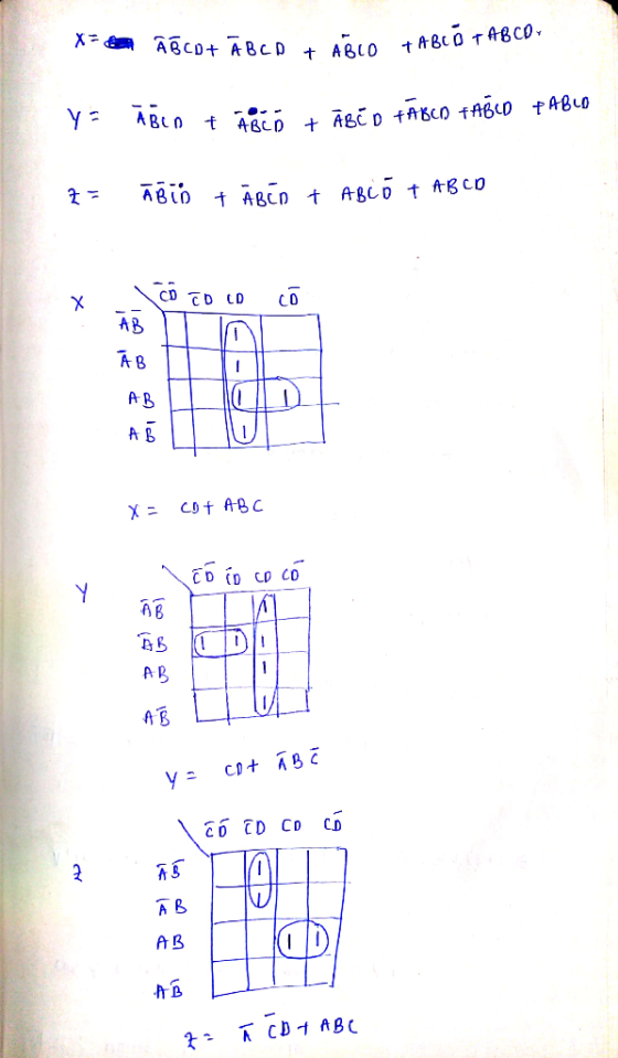
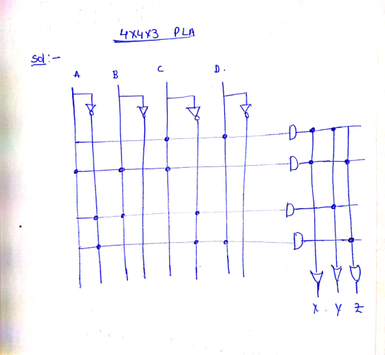
1) Implement the following equations using PLA: X=AB'D+A\c+BC+CD! Y=A\c'+AC+CD Z=CD+A/C +AB/D
 1) Implement the following equations using PLA: X=AB'D+A\c+BC+CD! Y=A\c'+AC+CD Z=CD+A/C +AB/D
Tabulate the truth table for an 8x4 ROM that implements the Boolean functions. (a) A(X, Y,...
Tabulate the truth table for an 8x4 ROM that implements the Boolean functions. (a) A(X, Y, Z) = Σm(1, 2, 4) (b) B(X, Y, Z) = Σm(3, 5, 7) (c) C(X, Y, Z) = Σm(1, 2, 6, 7) (d) D(X, Y, Z) = Σm(2, 3, 5, 6, 7)
 3. (25%) Implement the following 3 functions W,X,Y on a PLA with 4 product terms (Use common terms to optimize the design to obtain 4 or less terms) W(A, B, C) = X(A, B, C) = Y(A, B, C) = m(0, 1,4,5) m(3,4,5) m(0, 1, 2, 3)
 3. (25%) Implement the following 3 functions W,X,Y on a PLA with 4 product terms (Use common terms to optimize the design to obtain 4 or less terms) W(A, B, C) = X(A, B, C) = Y(A, B, C) = m(0, 1, 4, 5) m(3, 4, 5) m(0, 1, 2, 3)
 Computer architecture
Having the next Boolean functions: F1(x,y,z)-П (1, 3, 5) . F2(x,y,z)-Σ (0, 2, 4, 5) . 1. Make one logic gate design circuit, using AND, OR and NOT logic gates (20 points). 2. Design two 4-to-1 selectors, one for each Boolean function (20 points) 3. Design one 3-to-8 decoder to solve both Boolean functions (20 points) 4. Design a 8x2 ROM to solve both Boolean functions (20 points) 5. Design a 3x5x2 PLA to solve both Boolean functions...
Computer architecture
Having the next Boolean functions: F1(x,y,z)-П (1, 3, 5) . F2(x,y,z)-Σ (0, 2, 4, 5) . 1. Make one logic gate design circuit, using AND, OR and NOT logic gates (20 points). 2. Design two 4-to-1 selectors, one for each Boolean function (20 points) 3. Design one 3-to-8 decoder to solve both Boolean functions (20 points) 4. Design a 8x2 ROM to solve both Boolean functions (20 points) 5. Design a 3x5x2 PLA to solve both Boolean functions...
 7. Memory. A ROM chip with a size of 8 words by 4 bits is shown in the figure below. Please use this ROM chip, implement the following four logic functions by using the dot-notation. You can mark a dot to indicate that particular cell stores a value of 1. Note: in the following figure, A is the least significant bit of the address input. (10 points) F1= ABC +A C F2= ABC +BC F3= AC + B F4- ABC...
 1) Implement the following equations using PLA: X=AB'D+A\c+BC+CD! Y=A\c'+AC+CD Z=CD+A/C +AB/D
Most questions answered within 3 hours.
-
Write a psudocode:
1. Define a function called authorize that takes in 2 strings,
uName, and...
asked 1 minute from now -
What mass of ethylene glycol (C2H6O2) must be added to 211.0 g
of water to obtain...
asked 2 seconds from now -
Mary's employer has a defined benefits retirement plan, which
pay 3.2% of her last year's salary...
asked 3 minutes ago -
What are the characteristics and behavior of an ethical
manager?
Explain, in your words, what ethics...
asked 19 minutes ago -
1. Which of the following is NOT an argument that McMahan uses
to show that jus...
asked 41 minutes ago -
A crate slides up a frictionless slope. At the end of 3 seconds
its velocity is...
asked 58 minutes ago -
Use the following information to answer the next seven
questions.
Suppose there are three potential states...
asked 54 minutes ago -
If we only have interstitial and substitutional diffusion, then
what do we consider the process of...
asked 1 hour ago -
You look at yourself in a shiny 9.6-cm-diameter Christmas tree
ball.
If your face is 21.0...
asked 1 hour ago -
If we were to measure the relaxation time of a muscle after
undergoing tetanus compared to...
asked 1 hour ago -
4CO(g) + 8H2(g) -----> 3CH4(g) +
CO2(g) + 2H2O(l)
Use the following data as needed to...
asked 1 hour ago -
without using map
1. Write a C++ program to find out the top 10 words in...
asked 1 hour ago