program an 8-to-1 multiplexor using verilog
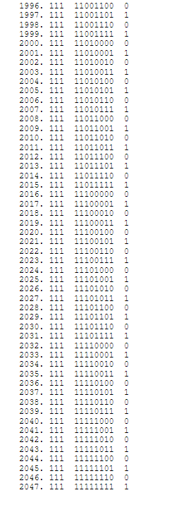
output of time table from 1 - 2047
For example output should look like....
--------- [Start of table] ---------------------------- [End of table] ----------

Here is example of 4x1 Multiplexor ... Just need code for 8x1 Multiplexor
module DecoderMod(s, o);
input [1:0] s;
output [0:3] o;
wire [1:0] inv_s;
not(inv_s[1], s[1]);
not(inv_s[0], s[0]);
and(o[0], inv_s[1], inv_s[0]);
and(o[1], inv_s[1], s[0]);
and(o[2], s[1], inv_s[0]);
and(o[3], s[1], s[0]);
endmodule
module MuxMod(s, d, o);
input [1:0] s;
input [0:3] d;
output o;
wire [0:3] s_decoded, and_out;
DecoderMod my_decoder(s, s_decoded);
and(and_out[0], d[0], s_decoded[0]);
and(and_out[1], d[1], s_decoded[1]);
and(and_out[2], d[2], s_decoded[2]);
and(and_out[3], d[3], s_decoded[3]);
or(o, and_out[0], and_out[1], and_out[2], and_out[3]);
endmodule
module TestMod;
reg [1:0] s;
reg [0:3] d;
wire o;
MuxMod my_mux(s, d, o);
initial begin
$display("Time s. d... o");
$display("---- -- ---- -");
$monitor("%4d %b %b %b", $time, s, d, o);
end
always begin d[3] = 0; #1; d[3] = 1; #1; end
always begin d[2] = 0; #2; d[2] = 1; #2; end
always begin d[1] = 0; #4; d[1] = 1; #4; end
always begin d[0] = 0; #8; d[0] = 1; #8; end
always begin s[0] = 0; #16; s[0] = 1; #16; end
always begin s[1] = 0; #32; s[1] = 1; #32; end
initial #63 $finish; // terminates after 63 cycles
endmodule
Homework Answers
- module mux8to1( Out,
- Sel,
- In1,
- In2,
- In3,
- In4,
- In5,
- In6,
- In7,
- In8
- );
- input [7:0] In1,
- In2,
- In3,
- In4,
- In5,
- In6,
- In7,
- In8; //The eight 8-bit input lines of the Mux
- input [2:0] Sel; //The three bit selection line
- output [7:0] Out; //The single 8-bit output line of the Mux
- reg [7:0] Out;
- //Check the state of the input lines
- always @ (In1 or In2 or In3 or In4 or In5 or In6 or In7 or In8 or Sel)
- begin
- case (Sel)
- 3'b000 : Out = In1;
- 3'b001 : Out = In2;
- 3'b010 : Out = In3;
- 3'b011 : Out = In4;
- 3'b100 : Out = In5;
- 3'b101 : Out = In6;
- 3'b110 : Out = In7;
- 3'b111 : Out = In8;
- default : Out = 8'bx;
- //If input is undefined then output is undefined
- endcase
- end
- endmodule
Add Answer to:
program an 8-to-1 multiplexor using verilog
output of time table from 1 - 2047
For example...
Write Verilog modules: a 3x8 decoder and a 8x1 multiplexor. The multiplexor “includes” the decoder module...
Write Verilog modules: a 3x8 decoder and a 8x1 multiplexor. The multiplexor “includes” the decoder module as part of it. Use arrays as much as possible. EXAMPLE: module DecoderMod(s, o); // module definition input s; output [0:1] o; not(o[0], s); assign o[1] = s; endmodule module MuxMod(s, d, o); input s; input [0:1] d; output o; wire [0:1] s_decoded, and_out; DecoderMod my_decoder(s, s_decoded); // create instance and(and_out[0], d[0], s_decoded[0]); and(and_out[1], d[1], s_decoded[1]); or(o, and_out[0], and_out[1]); endmodule
why its 4-to-1 mux behavioral? What does the logic circuit represented by the following Verilog module...
 why its 4-to-1 mux behavioral?
What does the logic circuit represented by the following Verilog module do, and what Verilog description style does it use? // My Verilog module #1 module mymodl ( x, d, q) input[1:0] x;input[3:0] d;output q; reg q; wire [1:0] x; wire [3:0] d; always ( x or d) begin case ( x ) 1 : q=d[1]; 2 : g=d[2]; 3 q d[3]; endcase end endmodule
why its 4-to-1 mux behavioral?
What does the logic circuit represented by the following Verilog module do, and what Verilog description style does it use? // My Verilog module #1 module mymodl ( x, d, q) input[1:0] x;input[3:0] d;output q; reg q; wire [1:0] x; wire [3:0] d; always ( x or d) begin case ( x ) 1 : q=d[1]; 2 : g=d[2]; 3 q d[3]; endcase end endmodule
7. Which of the following Verilog code segments will generate errors when compiled? A. module demo...
 7. Which of the following Verilog code segments will generate errors when compiled? A. module demo output reg F, input a): ire b; reg c assign b-c; initial begin end endmodule module demo5 output reg F, input reg a); ire b reg c assign bC; initial begin end C. module demooutput reg F, input wire a ire b reg c assign b c; initial begin F c& b; end D. O both A) and C) E. O none will generate...
Question 3: Realize the circuit below using Verilog. Include a signal “reset_n” for asynchronously clearing the...
 Question 3: Realize the circuit below using Verilog. Include a signal “reset_n” for asynchronously clearing the flip-flop. What type of circuit is this? Complete the following Verilog code. Write a test bench to test it. clk sel module aff (clk, reset_n, sel, q); input clk ; // Declare the inputs and outputs of the module. input reset_n; input sel; output q; reg q; wire D; ; // model the combinational logic assign D= always @( begin if ( else end...
a Read the following codes in Verilog and the corresponding testbench file. Describe what the codes...
a Read the following codes in Verilog and the corresponding testbench file. Describe what the codes are doing by adding comments in the code. Then write down the simulation results of res1, res2, res3, and res4, respectively. Source code module vector_defn (num1, res1, res2, res3, res4); input [7:0] num1; output res1; output [3:0] res2; output [0:7] res3; output [15:0] res4; assign res1=num1[2]; assign res2=num1[7:4]; assign res3=num1; assign res4={2{num1}}; endmodule testbench: `timescale 1ns / 1ps module vector_defn_tb; reg [7:0] in1; wire...
Using Verilog, write a simulation code that shows the function g(w, x, y, z) = wxyz...
Using Verilog, write a simulation code that shows the function g(w, x, y, z) = wxyz + w’x’y’z+w’x’yz’+w’xy’z’+wx’y’z’ using a 4 to 16 decoder that is built with two 3 to 8 decoders. The 3 to 8 source code I'm using is: module Dec3to8( input[2:0] A, input E, output[7:0] D ); assign D[0] = E & ~A[2] & ~A[1] & ~A[0]; assign D[1] = E & ~A[2] & ~A[1] & A[0]; assign D[2]...
(15 pts) 1. Draw a logic diagram for the Verilog code. module Seq_Ckt ( CLK, PR,...
 (15 pts) 1. Draw a logic diagram for the Verilog code. module Seq_Ckt ( CLK, PR, sel, Q); input CLK, PR, sel; output reg [2:0] Q; reg [2:0] y; assign Q = y; always @ (posedge PR, posedge CLK) begin if (PR== 1) then y <= 3'b111; else if (sel) begin y[2] <= y[1] ^ y[0]; y[1] <= y[2]; y[1]; end else y[2] <= y[2] ; y[1] <= y[1]; y[0]; y[O] <= y[0] <= end endmodule
I need the following in verilog. Attached is also the test bench. CODE // Design a...
I need the following in verilog. Attached is also the test bench. CODE // Design a circuit that divides a 4-bit signed binary number (in) // by 3 to produce a 3-bit signed binary number (out). Note that // integer division rounds toward zero for both positive and negative // numbers (e.g., -5/3 is -1). module sdiv3(out, in); output [2:0] out; input [3:0] in; endmodule // sdiv3 TEST BENCH module test; // these are inputs to "circuit under test" reg...
Write a testbench for use in Quartus' ModelSim Altera in verilog for the following code of...
Write a testbench for use in Quartus' ModelSim Altera in verilog for the following code of a 4x16 register: module regFile4x16 (input clk, input write, input [2:0] wrAddr, input [15:0] wrData, input [2:0] rdAddrA, output [15:0] rdDataA, input [2:0] rdAddrB, output [15:0] rdDataB); reg [15:0] reg0, reg1, reg2, reg3; assign rdDataA = rdAddrA == 0 ? reg0 : rdAddrA == 1 ? reg1 : rdAddrA == 2 ? reg2 : rdAddrA == 3...
I need a test bench code for this module in verilog. Verilog Code module part6 (А.В.us,G,E,L);...
 I need a test bench code for this module in
verilog.
Verilog Code module part6 (А.В.us,G,E,L); AlL ((Al --AI --op AIL (us) I-AIL input [2:0]A,B; input us; output G,E.I; reg G,E,L wire [2:0] A,B; always@(A or B) if (us 1)//unsigned mode begin しくーAB: //А is less G-A>B; //B is less 区-A-B; //logical (A equality end --oper AlL1 A[0] & -AIL E<-Ssigned(A) Ssigned(B); //logical equality opera AIL1I -AILI -operat else //signed mode begin しく=$signed(A)<$signed(B); //Ais less G-Ssigned(A)>Ssigned(B);: //B is less end...
I need a test bench code for this module in
verilog.
Verilog Code module part6 (А.В.us,G,E,L); AlL ((Al --AI --op AIL (us) I-AIL input [2:0]A,B; input us; output G,E.I; reg G,E,L wire [2:0] A,B; always@(A or B) if (us 1)//unsigned mode begin しくーAB: //А is less G-A>B; //B is less 区-A-B; //logical (A equality end --oper AlL1 A[0] & -AIL E<-Ssigned(A) Ssigned(B); //logical equality opera AIL1I -AILI -operat else //signed mode begin しく=$signed(A)<$signed(B); //Ais less G-Ssigned(A)>Ssigned(B);: //B is less end...
 why its 4-to-1 mux behavioral?
What does the logic circuit represented by the following Verilog module do, and what Verilog description style does it use? // My Verilog module #1 module mymodl ( x, d, q) input[1:0] x;input[3:0] d;output q; reg q; wire [1:0] x; wire [3:0] d; always ( x or d) begin case ( x ) 1 : q=d[1]; 2 : g=d[2]; 3 q d[3]; endcase end endmodule
why its 4-to-1 mux behavioral?
What does the logic circuit represented by the following Verilog module do, and what Verilog description style does it use? // My Verilog module #1 module mymodl ( x, d, q) input[1:0] x;input[3:0] d;output q; reg q; wire [1:0] x; wire [3:0] d; always ( x or d) begin case ( x ) 1 : q=d[1]; 2 : g=d[2]; 3 q d[3]; endcase end endmodule
 7. Which of the following Verilog code segments will generate errors when compiled? A. module demo output reg F, input a): ire b; reg c assign b-c; initial begin end endmodule module demo5 output reg F, input reg a); ire b reg c assign bC; initial begin end C. module demooutput reg F, input wire a ire b reg c assign b c; initial begin F c& b; end D. O both A) and C) E. O none will generate...
 Question 3: Realize the circuit below using Verilog. Include a signal “reset_n” for asynchronously clearing the flip-flop. What type of circuit is this? Complete the following Verilog code. Write a test bench to test it. clk sel module aff (clk, reset_n, sel, q); input clk ; // Declare the inputs and outputs of the module. input reset_n; input sel; output q; reg q; wire D; ; // model the combinational logic assign D= always @( begin if ( else end...
 (15 pts) 1. Draw a logic diagram for the Verilog code. module Seq_Ckt ( CLK, PR, sel, Q); input CLK, PR, sel; output reg [2:0] Q; reg [2:0] y; assign Q = y; always @ (posedge PR, posedge CLK) begin if (PR== 1) then y <= 3'b111; else if (sel) begin y[2] <= y[1] ^ y[0]; y[1] <= y[2]; y[1]; end else y[2] <= y[2] ; y[1] <= y[1]; y[0]; y[O] <= y[0] <= end endmodule
 I need a test bench code for this module in
verilog.
Verilog Code module part6 (А.В.us,G,E,L); AlL ((Al --AI --op AIL (us) I-AIL input [2:0]A,B; input us; output G,E.I; reg G,E,L wire [2:0] A,B; always@(A or B) if (us 1)//unsigned mode begin しくーAB: //А is less G-A>B; //B is less 区-A-B; //logical (A equality end --oper AlL1 A[0] & -AIL E<-Ssigned(A) Ssigned(B); //logical equality opera AIL1I -AILI -operat else //signed mode begin しく=$signed(A)<$signed(B); //Ais less G-Ssigned(A)>Ssigned(B);: //B is less end...
I need a test bench code for this module in
verilog.
Verilog Code module part6 (А.В.us,G,E,L); AlL ((Al --AI --op AIL (us) I-AIL input [2:0]A,B; input us; output G,E.I; reg G,E,L wire [2:0] A,B; always@(A or B) if (us 1)//unsigned mode begin しくーAB: //А is less G-A>B; //B is less 区-A-B; //logical (A equality end --oper AlL1 A[0] & -AIL E<-Ssigned(A) Ssigned(B); //logical equality opera AIL1I -AILI -operat else //signed mode begin しく=$signed(A)<$signed(B); //Ais less G-Ssigned(A)>Ssigned(B);: //B is less end...
Most questions answered within 3 hours.
-
In testing a new drug, researchers found that 5% of all patients
using it will have...
asked 24 minutes ago -
List the six general types of information management systems,
and give one logistics application to each...
asked 15 minutes ago -
XYZ corporation uses statistical quality control to monitor the
quality of their product. They have determined...
asked 18 minutes ago -
If a liquid
contains 60% sugar and 40% water through out its composition then
what is...
asked 26 minutes ago -
The data in set A represents prices (with tax included) of a
large cup of regular...
asked 36 minutes ago -
How do neuropsychological assessments provide information about
impairment? How could this information be misused?
asked 28 minutes ago -
Define SNP and elaborate various type of SNPs and their
importance in pharmacogenetics?
asked 32 minutes ago -
Description
There are 4 classes, Figure is the base class,both Triangle,
Rectangle and Circle are all...
asked 33 minutes ago -
What will the standard deviation of these exam grades be? A
square bracket means inclusive, so...
asked 43 minutes ago -
Beginning Retained Earnings are $ 79 comma 000 $79,000; sales
are $ 31 comma 700 $31,700;...
asked 45 minutes ago -
Please explain/demonstrate how to use NLTK to test unigram,
bigram, and trigram character models on guessing...
asked 52 minutes ago -
what you feel is most important to you and why regarding your
typing skills?
asked 53 minutes ago