a) Although buried in the same semiconductor substrate, why the source and drain of a transistor...
a) Although buried in the same semiconductor substrate, why the source and drain of a transistor is electrically isolated when no external voltage is applied?
b) Why is it essential to connect the p-type substrate of a NMOS transistor to the least potential (usually ground) and the n-type substrate of a PMOS transistor to the highest potential (usually supply) for the MOSFET operation?
c) What is a threshold voltage? What happens to the drain current below threshold?
d) What isa pinch-off voltage? What happens to the drain current at pinch off?
e) A MOSFET is usually called a voltage controlled current source because the output current is controlled by voltage(s).
Identify the voltage (s) which control the flow of the drain current in the channel of a MOSFET?
Homework Answers
(a) Source and drain of the transistor is electrically isolated when no external voltage is applied:
- It is the electrical separation between various functional circuits in a system such that there is no direct conduction path available between them
- isolation may be necessary for functional purposes
- It provides protection against any fault on the high voltage side as the isolation barrier blocks electrical power from reaching the user in spite of component damage or failure.
(b) connect the p-type substrate of a NMOS transistor to the least potential (usually ground) and the n-type substrate of a PMOS transistor to the highest potential (usually supply) for the MOSFET operation :
- Cross section of NMOS and PMOS as shown below,

-
The first thing to notice is that the all of the substrate is p-doped. Beside the NMOS there is a terminal labeled B, with a p+ doping.
-
We understand p+ as a heavily p-doped semiconductor, which increases its conductivity. On the PMOS side, what you have is a n-doped well “n-well”), with a bias terminal connected.
-
When the correct voltage is applied to the gate, charge accumulation constructs a channel between the source and the drain.
That B terminal must be connected in such way to make a reverse diodes with the sources and drains of both transistors.
-
That means that in the NMOS, it will be connected to the lowest available potential, and in the PMOS, to the highest available potential.
-
These connections avoid the those drain and source terminals to conduct directly to the substrate, which would make the transistor act as a fixed resistor.

(c) threshold voltage:
- Threshold voltage is the voltage applied between gate and source of a MOSFET that is needed to turn the device on for linear and saturation regions of operation.
- drain current below threshold:
- the channel is "pinched off" so that no current can flow, even though there are charge carriers available.
(d) pinch-off voltage:
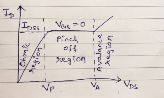
- the channel behaves as a semiconductor resistance, therefore it follows ohm's law. The region is called ohmic region, with increasing current, the ohmic voltage drop between the source and the channel region reverse biased the junction, the conducting portion of the channel begins to constrict and ID begins to level off until a specific value of VDS is reached, called the pinch of voltage VP
- the drain current reaches at the pinch-off potential, and saturates which can be shown in above figure.

Add Answer to:
a) Although buried in the same semiconductor substrate, why the
source and drain of a transistor...
3. In N-MOSFET transistor, the transistor is manufactured on top ....... substrate. In the triode mode,...
 3. In N-MOSFET transistor, the transistor is manufactured on top ....... substrate. In the triode mode, the channel between the source and drain are ......... channel a) P-type and N-type b) N-type and N-type c) P-type and P-type d) N-type and P-type , what is the base bias voltage? 4. If VCC = +18 V, voltage-divider resistor R1 is 4.7 k2, and R2 is 1500 a) 8.6 V b) 4.35 V c) 2.90 V d) 0.7 V 5. The ends...
2. (25 pts) An NMOS transistor operating in the linearregion with VDs 50mV is measured to...
 2. (25 pts) An NMOS transistor operating in the linearregion with VDs 50mV is measured to have a drain current of 25μΑ for VGs* IV (Case I) and 50μΑ for VGs* 1.5V (Case II). a. (5 pts) Calculate the threshold voltage ofthe NMOS transistor b. (5 pts) Calculate the resistance between drain and source for each case c. (5 pts) Calculate the device aspect ratio W/L iKn_ 50μΑ/. d. (5 pts) Calculate the drain current of the NMOS transistor if...
3. A PMOS transistor has the gate and drain tied together. The source voltage is V-SV,...
 3. A PMOS transistor has the gate and drain tied together. The source voltage is V-SV, drain voltage VD-2V, threshold voltage Vrp--2v. μ.Cgox-8 μΑ/V2 and L-10μm . The transistor supports a current of Isp a) Calculate the width of the transistor W and gate oxide thickness tgox Note: μ,-480 cm 2/(V-s) and Ego, (relative permittivity of Si02-39 b) Using a scaling factor S-5, if only the length L is scaled by 1/S with all other parameters remaining the same, calculate...
1.24P)a) Plot the structure of p-channel MOS-FET (Show semiconductor structure, gate, drain, source and voltage polarities)...
 1.24P)a) Plot the structure of p-channel MOS-FET (Show semiconductor structure, gate, drain, source and voltage polarities) and summarize the working principle. b) Explain what happens if you change drain source voltage polarity. c) Plot the band diagram, approximate distributions of charge, electric field, and electrostatic potential in the ideal MOS capacitor in inversion for the p-channel case.
3) AMOS Assume a mon I V. 2 V.V2V threshold voltage of 0.7 V. The transistor...
 3) AMOS Assume a mon I V. 2 V.V2V threshold voltage of 0.7 V. The transistor is in c Sammation ut off d. Not sufficient information since substrate and source are at different voltage levels None of the above 4) Choose the best answer regarding channel length modulation effect Results in lower drain current b. Increases absolute value of the threshold voltage thru body effect Depletion region effectively shortens the channel length d. Makes drain current depend on drain voltage...
all please TEST #3 of the FET and are unaffected by 1. Schokley's equation defines the...
 all please
TEST #3 of the FET and are unaffected by 1. Schokley's equation defines the the network in which the device is employed. (a) Vas characteristics (b) drain characteristics (c) input output characteristics (d) transfer characteristics 2. For an N-channel JFET Ipss -8 mA and Vp-6 V. If Vas-2 V then what is the value of the drain current ID? (a) 2.666 mA (b) 3.5 LA (c) 3.55 mA (d) 5.33 mA 3. D-MOSFETs can operate in: (a) The...
all please
TEST #3 of the FET and are unaffected by 1. Schokley's equation defines the the network in which the device is employed. (a) Vas characteristics (b) drain characteristics (c) input output characteristics (d) transfer characteristics 2. For an N-channel JFET Ipss -8 mA and Vp-6 V. If Vas-2 V then what is the value of the drain current ID? (a) 2.666 mA (b) 3.5 LA (c) 3.55 mA (d) 5.33 mA 3. D-MOSFETs can operate in: (a) The...
An n-channel Sí MOSFET (ni-1.5 1010 cm-3 ,er-11.8) with 50 nm thick HfO2 high- K dielectric...
 An n-channel Sí MOSFET (ni-1.5 1010 cm-3 ,er-11.8) with 50 nm thick HfO2 high- K dielectric (Er-25). The device width is W-10 m wide. The distance between the source and drain is L 0.5 μm long. The diffusion constant of the minority carriers in the channel at room temperature is 25 cm2/s. The n+ poly-Si gate is doped with Np 1020 cm-3 donors. This MOSFET is designed to have a threshold voltage of Vt 0.5 V. A gate-source voltage of...
Q2 MOSFET and I-V Curves (Total 30 pts) Q2.1 Consider the band diagrams (conduction band) of...
 Q2 MOSFET and I-V Curves (Total 30 pts) Q2.1 Consider the band diagrams (conduction band) of a N-MOSFET along the channel (x) direction as shown in fig. 1. In fig. 1, the solid curve shows the band diagram with the gate voltage VG = 0. All the variables have their usual meaning. Which of the dashed curves (case I or case II) in fig. 1 represents of the band diagram (conduction band) of the N-MOSFET with VG >0? 5 pts...
1.30P)a) Plot the channel formation of p-channel MOS-FET for linear and saturation pinch-off regime (Kitabı referans...
 1.30P)a) Plot the channel formation of p-channel MOS-FET for linear and saturation pinch-off regime (Kitabı referans alınız, final cevap anahtarından farklı olabilir). Explain how the channel changes with applied voltages. Show semiconductor structure, gate, drain, source and voltage polarities. b) Explain what happens if you apply voltages like i.Vg <<0, Vd<<0, Vs=0; ii. Vg <<0, Vd >0, Vs=0, iii. Vg>0, Vd <0, Vs=0 to ideal MOS-FET structure (g:gate, s:source, d:drain). Explain clearly by referring to MOSFET structure (burada kanal ile...
 3. In N-MOSFET transistor, the transistor is manufactured on top ....... substrate. In the triode mode, the channel between the source and drain are ......... channel a) P-type and N-type b) N-type and N-type c) P-type and P-type d) N-type and P-type , what is the base bias voltage? 4. If VCC = +18 V, voltage-divider resistor R1 is 4.7 k2, and R2 is 1500 a) 8.6 V b) 4.35 V c) 2.90 V d) 0.7 V 5. The ends...
 2. (25 pts) An NMOS transistor operating in the linearregion with VDs 50mV is measured to have a drain current of 25μΑ for VGs* IV (Case I) and 50μΑ for VGs* 1.5V (Case II). a. (5 pts) Calculate the threshold voltage ofthe NMOS transistor b. (5 pts) Calculate the resistance between drain and source for each case c. (5 pts) Calculate the device aspect ratio W/L iKn_ 50μΑ/. d. (5 pts) Calculate the drain current of the NMOS transistor if...
 3. A PMOS transistor has the gate and drain tied together. The source voltage is V-SV, drain voltage VD-2V, threshold voltage Vrp--2v. μ.Cgox-8 μΑ/V2 and L-10μm . The transistor supports a current of Isp a) Calculate the width of the transistor W and gate oxide thickness tgox Note: μ,-480 cm 2/(V-s) and Ego, (relative permittivity of Si02-39 b) Using a scaling factor S-5, if only the length L is scaled by 1/S with all other parameters remaining the same, calculate...
 1.24P)a) Plot the structure of p-channel MOS-FET (Show semiconductor structure, gate, drain, source and voltage polarities) and summarize the working principle. b) Explain what happens if you change drain source voltage polarity. c) Plot the band diagram, approximate distributions of charge, electric field, and electrostatic potential in the ideal MOS capacitor in inversion for the p-channel case.
 1.24P)a) Plot the structure of p-channel MOS-FET (Show semiconductor structure, gate, drain, source and voltage polarities) and summarize the working principle. b) Explain what happens if you change drain source voltage polarity. c) Plot the band diagram, approximate distributions of charge, electric field, and electrostatic potential in the ideal MOS capacitor in inversion for the p-channel case.
 3) AMOS Assume a mon I V. 2 V.V2V threshold voltage of 0.7 V. The transistor is in c Sammation ut off d. Not sufficient information since substrate and source are at different voltage levels None of the above 4) Choose the best answer regarding channel length modulation effect Results in lower drain current b. Increases absolute value of the threshold voltage thru body effect Depletion region effectively shortens the channel length d. Makes drain current depend on drain voltage...
 all please
TEST #3 of the FET and are unaffected by 1. Schokley's equation defines the the network in which the device is employed. (a) Vas characteristics (b) drain characteristics (c) input output characteristics (d) transfer characteristics 2. For an N-channel JFET Ipss -8 mA and Vp-6 V. If Vas-2 V then what is the value of the drain current ID? (a) 2.666 mA (b) 3.5 LA (c) 3.55 mA (d) 5.33 mA 3. D-MOSFETs can operate in: (a) The...
all please
TEST #3 of the FET and are unaffected by 1. Schokley's equation defines the the network in which the device is employed. (a) Vas characteristics (b) drain characteristics (c) input output characteristics (d) transfer characteristics 2. For an N-channel JFET Ipss -8 mA and Vp-6 V. If Vas-2 V then what is the value of the drain current ID? (a) 2.666 mA (b) 3.5 LA (c) 3.55 mA (d) 5.33 mA 3. D-MOSFETs can operate in: (a) The...
 An n-channel Sí MOSFET (ni-1.5 1010 cm-3 ,er-11.8) with 50 nm thick HfO2 high- K dielectric (Er-25). The device width is W-10 m wide. The distance between the source and drain is L 0.5 μm long. The diffusion constant of the minority carriers in the channel at room temperature is 25 cm2/s. The n+ poly-Si gate is doped with Np 1020 cm-3 donors. This MOSFET is designed to have a threshold voltage of Vt 0.5 V. A gate-source voltage of...
 Q2 MOSFET and I-V Curves (Total 30 pts) Q2.1 Consider the band diagrams (conduction band) of a N-MOSFET along the channel (x) direction as shown in fig. 1. In fig. 1, the solid curve shows the band diagram with the gate voltage VG = 0. All the variables have their usual meaning. Which of the dashed curves (case I or case II) in fig. 1 represents of the band diagram (conduction band) of the N-MOSFET with VG >0? 5 pts...
 1.30P)a) Plot the channel formation of p-channel MOS-FET for linear and saturation pinch-off regime (Kitabı referans alınız, final cevap anahtarından farklı olabilir). Explain how the channel changes with applied voltages. Show semiconductor structure, gate, drain, source and voltage polarities. b) Explain what happens if you apply voltages like i.Vg <<0, Vd<<0, Vs=0; ii. Vg <<0, Vd >0, Vs=0, iii. Vg>0, Vd <0, Vs=0 to ideal MOS-FET structure (g:gate, s:source, d:drain). Explain clearly by referring to MOSFET structure (burada kanal ile...
Most questions answered within 3 hours.
-
Does direct Medicare reimbursement of Advanced practice nurses
increase access to their services?
asked 1 minute from now -
List and explain why a company would choose to use a
published
compensation survey vs. creating...
asked 9 minutes ago -
A discrete random variable X can take values from 1 to 10. Find
the variance of...
asked 22 minutes ago -
The primary financial goal of a corporation is to maximize:
shareholders wealth.
earnings per share.
stock...
asked 29 minutes ago -
determine whether the vectors u=(1,2,3,), v=(-2,1,0) and
w=(1,0,1) are linearly dependent or independent.
asked 35 minutes ago -
python
Define a function called print_values which takes a dictionary
object as a parameter. The function...
asked 1 hour ago -
In Chapter 1 you created a program named Triangle in
which you displayed a seven-line triangle...
asked 1 hour ago -
Research question: What are the differences between separately
stated and non separately stated transactions in an...
asked 1 hour ago -
By using Arduino write a code that connects two LEDs to two
push-buttons. Each button controls...
asked 2 hours ago -
Bank of America has bonds that pay a coupon interest rate of 5.5
percent and mature...
asked 3 hours ago -
Problem: Patient Fees C++
You are to write a program that computes a patient’s bill for...
asked 5 hours ago -
In a population of interest, we know that, 77% drink coffee, and
23% drink tea. Assume...
asked 5 hours ago