
Homework Answers

Add Answer to:
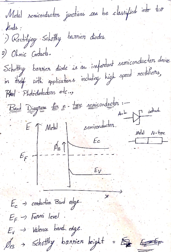
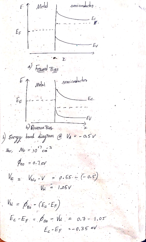
Problem 7: MS contact n-type Si Consider a contact between NiSi and n-type silicon with N 10 cm m...
2. Design a Schottky Contact with N-type Silicon a. b. c. Identify a metal that farms a Schottky ...
 2. Design a Schottky Contact with N-type Silicon a. b. c. Identify a metal that farms a Schottky Contact at 0V bias Sketch the Band-bending diagram a 0V bias Sketch the Band-bending diagram for Forward Bias and Reverse Bias, label the polarity of bias. ypes ot Metal-Semiconductor Contacts Metal Metal N-type implies electrons are the majority Conduction band determines MS junction behavior type implies holes are the majority Valence band determines MS junction behavior . . N-type Schottky P-type Schottky...
2. (20 pts) - A Silicon sample doped n-type with Nd = 5x10 cm has an...
 2. (20 pts) - A Silicon sample doped n-type with Nd = 5x10 cm has an ideal Schottky barrier formed on its surface. The Silicon electron affinity is 4.0 eV, and the Silicon bandgap is 1.1 eV. The metal work function is 4.7 eV. Draw the equilibrium band diagram and for the reverse bias diagram with Vr = 3 V. In each diagram show the numerical values for OB, Vo , (Vo + Vr), EFs - Ej, Ec-EFs, and qVr
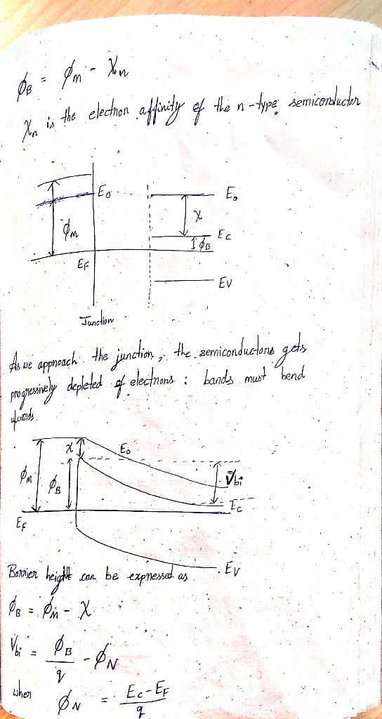
An ideal metal-semiconductor (M-S) junction is formed on the n-type Si semiconductor that is uniformly doped...
 An ideal metal-semiconductor (M-S) junction is formed on the n-type Si semiconductor that is uniformly doped with a donor impurity (phosphorus) concentration of 1016 cm. The metal work function is 4.5 eV, and the Si electron affinity is 4 eV. Assuming that this M-S junction is at 300K, give your best answers to the following questions. (50 points) (a) At thermal equilibrium, draw the energy band diagram including meaningful parameters (energy barriers, energy levels, depletion width, etc.). (b) Calculate the...
Problem 3: MS contact -Vcharacteristics A Schottky diode maintained at T 300K is formed between TiSiz and silicon d...
 Problem 3: MS contact -Vcharacteristics A Schottky diode maintained at T 300K is formed between TiSiz and silicon doped with 101 cm3 phosphorus. The cross-sectional area is 100 μm 100pm-104 cm, a) Determine the reverse saturation current Is, using the measured value of Schottky barrier height given in Lecture Note. Recall from Lecture Note that the conductivity effective masses for electrons and holes in silicon are 0.26mo and 0.39mo, respectively b) Plot the forward-bias diode I-Vcharacteristic on a log-linear scale...
A metal, with a work function Ф,,-41 V, is deposited on an n-type silicon semiconductor with elec...
 A metal, with a work function Ф,,-41 V, is deposited on an n-type silicon semiconductor with electron affinity 4.0V and energy bandgap 1.12eV. Assuming no interface states exist at the junction and operation temperature at 300K. Effective density of states in conduction band (N 3.22 x 10 cm3. Effective density of states in valence band (N) 1.83 x 10" cm 193 A) Sketch the energy band diagram for zero bias for the case when no space charge region exists at...
1. Draw the band diagram of Schottky and Ohmic contact at metal/n-type silicon. Explain why ohmic...
 1. Draw the band diagram of Schottky and Ohmic contact at metal/n-type silicon. Explain why ohmic contact cannot be formed using common metals
1. A metal/n-GaAs Schottky Barrier is formed by depositing platinum on n-GaAs. The electron affinity of...
1. A metal/n-GaAs Schottky Barrier is formed by depositing platinum on n-GaAs. The electron affinity of GaAs is 4.0 eV. The work function of Pt is 5.0 eV. The doping in GaAs is 1E16/cm3, and Nc=5E17/cm3. i) Draw the thermal equilibrium energy band diagram for the structure ii) Calculate the barrier height and the built-in voltage iii) Calculate the depletion width in GaAs, given ε(total) for GaAs=1E-12 F/cm --> w=sqrt((2*ε*Vbi)/(q*ND)) iv) Calculate the depletion capacitance for 1 cm2 area v)...
All needed data is given. Kindly solve all parts of the problem (CLEARLY).. assume ni = 1x10^10 i...
 All needed data is given. Kindly solve all parts of the
problem (CLEARLY).. assume ni = 1x10^10 if needed
3) Answer the follow questions about a Metal-Silicon MS junctions. Assume a hypothetical metal with a workfunction of Фм-4.60 eV. Assume that the electron affinity of Si is-4.03 eV 3a) Assume that the Si is N-type with N 3b) 3c) 3d) 10and draw an energy band diagram. Indicate the Schottky barrier height on your sketch Assume that the Si is P-type...
All needed data is given. Kindly solve all parts of the
problem (CLEARLY).. assume ni = 1x10^10 if needed
3) Answer the follow questions about a Metal-Silicon MS junctions. Assume a hypothetical metal with a workfunction of Фм-4.60 eV. Assume that the electron affinity of Si is-4.03 eV 3a) Assume that the Si is N-type with N 3b) 3c) 3d) 10and draw an energy band diagram. Indicate the Schottky barrier height on your sketch Assume that the Si is P-type...
B2 Consider a diode formed by making a p-n junction structure in a silicon sample as shown in Fig. B2. nt laver p-type...
 B2 Consider a diode formed by making a p-n junction structure in a silicon sample as shown in Fig. B2. nt laver p-type Si Fig. B2 (a). If the dopant concentrations of the n layer and the p-type silicon are 6x101" cm and 8x10 cm respectively, calculate the built-in potential of the p-n junction at room temperature (300 K) 15 (3 marks) (b). Due to overheating of the silicon sample, the diode has an operation temperature of 200 °C and...
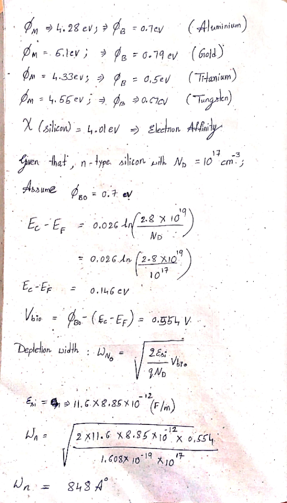
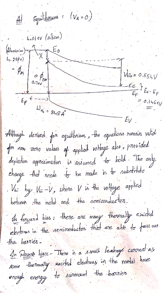
Find barrier height, built-in voltage, maximum E- field, and the depletion layer width at equilibrium for...
 Find barrier height, built-in voltage, maximum E- field, and the depletion layer width at equilibrium for W-Si (n-type) contact (tungsten silicide) Given: Φ,-4.55eV for WX(Si)-4.01 eV: Si doping - 1016 cm-3 Draw the band diagram at equilibrium. Required Constants: for silicon at T-300°K, ni-1010/cm3. The Boltzmann constant kg-k-8.61x10-eV/K. Silicon bandgap energy Ev-1.12 eV
 2. Design a Schottky Contact with N-type Silicon a. b. c. Identify a metal that farms a Schottky Contact at 0V bias Sketch the Band-bending diagram a 0V bias Sketch the Band-bending diagram for Forward Bias and Reverse Bias, label the polarity of bias. ypes ot Metal-Semiconductor Contacts Metal Metal N-type implies electrons are the majority Conduction band determines MS junction behavior type implies holes are the majority Valence band determines MS junction behavior . . N-type Schottky P-type Schottky...
 2. (20 pts) - A Silicon sample doped n-type with Nd = 5x10 cm has an ideal Schottky barrier formed on its surface. The Silicon electron affinity is 4.0 eV, and the Silicon bandgap is 1.1 eV. The metal work function is 4.7 eV. Draw the equilibrium band diagram and for the reverse bias diagram with Vr = 3 V. In each diagram show the numerical values for OB, Vo , (Vo + Vr), EFs - Ej, Ec-EFs, and qVr
 An ideal metal-semiconductor (M-S) junction is formed on the n-type Si semiconductor that is uniformly doped with a donor impurity (phosphorus) concentration of 1016 cm. The metal work function is 4.5 eV, and the Si electron affinity is 4 eV. Assuming that this M-S junction is at 300K, give your best answers to the following questions. (50 points) (a) At thermal equilibrium, draw the energy band diagram including meaningful parameters (energy barriers, energy levels, depletion width, etc.). (b) Calculate the...
 Problem 3: MS contact -Vcharacteristics A Schottky diode maintained at T 300K is formed between TiSiz and silicon doped with 101 cm3 phosphorus. The cross-sectional area is 100 μm 100pm-104 cm, a) Determine the reverse saturation current Is, using the measured value of Schottky barrier height given in Lecture Note. Recall from Lecture Note that the conductivity effective masses for electrons and holes in silicon are 0.26mo and 0.39mo, respectively b) Plot the forward-bias diode I-Vcharacteristic on a log-linear scale...
 A metal, with a work function Ф,,-41 V, is deposited on an n-type silicon semiconductor with electron affinity 4.0V and energy bandgap 1.12eV. Assuming no interface states exist at the junction and operation temperature at 300K. Effective density of states in conduction band (N 3.22 x 10 cm3. Effective density of states in valence band (N) 1.83 x 10" cm 193 A) Sketch the energy band diagram for zero bias for the case when no space charge region exists at...
 1. Draw the band diagram of Schottky and Ohmic contact at metal/n-type silicon. Explain why ohmic contact cannot be formed using common metals
 All needed data is given. Kindly solve all parts of the
problem (CLEARLY).. assume ni = 1x10^10 if needed
3) Answer the follow questions about a Metal-Silicon MS junctions. Assume a hypothetical metal with a workfunction of Фм-4.60 eV. Assume that the electron affinity of Si is-4.03 eV 3a) Assume that the Si is N-type with N 3b) 3c) 3d) 10and draw an energy band diagram. Indicate the Schottky barrier height on your sketch Assume that the Si is P-type...
All needed data is given. Kindly solve all parts of the
problem (CLEARLY).. assume ni = 1x10^10 if needed
3) Answer the follow questions about a Metal-Silicon MS junctions. Assume a hypothetical metal with a workfunction of Фм-4.60 eV. Assume that the electron affinity of Si is-4.03 eV 3a) Assume that the Si is N-type with N 3b) 3c) 3d) 10and draw an energy band diagram. Indicate the Schottky barrier height on your sketch Assume that the Si is P-type...
 B2 Consider a diode formed by making a p-n junction structure in a silicon sample as shown in Fig. B2. nt laver p-type Si Fig. B2 (a). If the dopant concentrations of the n layer and the p-type silicon are 6x101" cm and 8x10 cm respectively, calculate the built-in potential of the p-n junction at room temperature (300 K) 15 (3 marks) (b). Due to overheating of the silicon sample, the diode has an operation temperature of 200 °C and...
 Find barrier height, built-in voltage, maximum E- field, and the depletion layer width at equilibrium for W-Si (n-type) contact (tungsten silicide) Given: Φ,-4.55eV for WX(Si)-4.01 eV: Si doping - 1016 cm-3 Draw the band diagram at equilibrium. Required Constants: for silicon at T-300°K, ni-1010/cm3. The Boltzmann constant kg-k-8.61x10-eV/K. Silicon bandgap energy Ev-1.12 eV
Most questions answered within 3 hours.
-
The manager at a car assembly plant believes that the mean
assembly time for a car...
asked 34 minutes ago -
Which of the following is true of electron capture?
A) It decreases the nuclide's mass number...
asked 2 hours ago -
Assuming an efficiency of 43.10%, calculate the actual yield of
magnesium nitrate formed from 114.9 g...
asked 2 hours ago -
The highly pathogenic bacterium Clostridium
perfringens causes gangrene, a disease that results in the
destruction of...
asked 4 hours ago -
In the context of situation analysis, which of the following is
a category for analysis in...
asked 4 hours ago -
In a study of the gas phase decomposition of sulfuryl chloride
at 600 K SO2Cl2(g)SO2(g) +...
asked 4 hours ago -
75 g of 2-propanol (C3H8O) and 25 g of pentane are mixed in a
200 mL...
asked 4 hours ago -
The 2800-turn coil in a dc motor has an area per turn of 1.1 ×
10-2...
asked 4 hours ago -
Draw a combinational logic circuit diagram with a symbol inside
the box for two I/P of...
asked 4 hours ago -
The cliché we use quite a lot in finance is: there is a need to
maximize...
asked 4 hours ago -
In class we discussed the addition of HCl to alpha pinene. Would
you expect one or...
asked 4 hours ago -
I'm trying to explain to my daughter to help her please help
me
I tagged the...
asked 4 hours ago