
Homework Answers


Add Answer to:
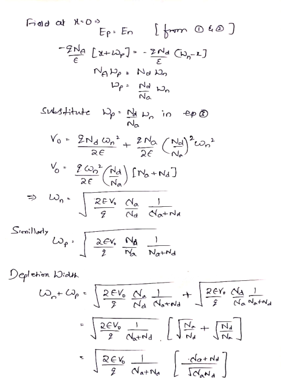
4. 16 points: For a pn diode, assume the donor concentration is Na, the acceptor concentration is...
3.13 Si pn junction Consider a long pn junction diode with an acceptor doping Naof 1018 cm-3 on t...
 3.13 Si pn junction Consider a long pn junction diode with an acceptor doping Naof 1018 cm-3 on the p-side and donor concentration of Nj on the n-side. The diode is forward biased and has a voltage of 0.6 V across it. The diode cross-sectional area is 1 mm2. The minority carrier recombination time, T, depends on the total dopant concentration, Ndopant (cm), through the following approximate empirical relation (5x 10⁻⁷)/(1 + 2 10-17N1°pan.) where T is in seconds. (a)...
3.13 Si pn junction Consider a long pn junction diode with an acceptor doping Naof 1018...
 3.13 Si pn junction Consider a long pn junction diode with an acceptor doping Naof 1018 cm-3 on the p-side and donor concentration of Nj on the n-side. The diode is forward biased and has a voltage of 0.6 V across it. The diode cross-sectional area is 1 mm2. The minority carrier recombination time, T, depends on the total dopant concentration, Ndopant (cm), through the following approximate empirical relation (5x 10⁻⁷)/(1 + 2 10-17N1°pan.) where T is in seconds. (a)...
THE REVERSE BIAS VOLTAGE APPLIED TO SILICON PN JUNCTION DIODE IS 4V, DOPING CONCENTRATION Na is...
THE REVERSE BIAS VOLTAGE APPLIED TO SILICON PN JUNCTION DIODE IS 4V, DOPING CONCENTRATION Na is 10^17 cm^-3, Nd = 10^16 cm^-3, ni = 1.3 x 10^9 cm^-3, temperature T = 273 k find the width of depletion region with the applied reverse voltage please check your answer that it is correct please it is a humble request
A pn iunction diode has the following parameters, Na-2x10^17 Dp 10.36 Tp - 5x10-'s Area is...
 A pn iunction diode has the following parameters, Na-2x10^17 Dp 10.36 Tp - 5x10-'s Area is 1mm 2 Nc-1x10 16 Dn-18.13 Tn-5x10-s Length of diode is 100 mm At equilibrium, what is the width of the depletion region, the built in potential, the electric field across the depletion region and the capacitance of the depletion region a. b. Can you tell from the doping levels which region the depletion regioin c. Find the Fermi level in both regions and the...
(iv) [2 Marks] A pn-junction has a built-in potential voltage of 1V across the junction. The width of the depletion reg...
 (iv) [2 Marks] A pn-junction has a built-in potential voltage of 1V across the junction. The width of the depletion region is 1um. The acceptor doping is NA 2 x 1015cm-3 in the P-side and a donor doping is Np = 8 x 1015cm-3 on the N-side. If the reference position x 0 is the edge of the depletion region on the P-side and the P region is on the left of the N region then where does the maximum...
Design an ideal abrupt silicon PN-junction at 300 K such that the donor impurity concentration in...
 XXX is 467
Design an ideal abrupt silicon PN-junction at 300 K such that the donor impurity concentration in the n-side N, = 5x1015 cm3 and the acceptor impurity concentration in the p-side N, = XXX × 1015/cm3 Assume that the diode area A-2x10⁻³ cm2 and 100cm work Note that the values obtained in the calculations may not be realistic as the Matric # varies greatly. The assignment is only to test your understanding, and must be handwritten Determine the...
XXX is 467
Design an ideal abrupt silicon PN-junction at 300 K such that the donor impurity concentration in the n-side N, = 5x1015 cm3 and the acceptor impurity concentration in the p-side N, = XXX × 1015/cm3 Assume that the diode area A-2x10⁻³ cm2 and 100cm work Note that the values obtained in the calculations may not be realistic as the Matric # varies greatly. The assignment is only to test your understanding, and must be handwritten Determine the...
Consider an abrupt p-n diode - made of an unknown semiconductor - in thermal equilibrium with...
Consider an abrupt p-n diode - made of an unknown semiconductor - in thermal equilibrium with as many donors in the n-type region as acceptors in the p-type region and a maximum electric field of -13 kV/cm and a total depletion layer width of 1 µm. (assume es/ e0 = 12) a) What is the applied voltage, Va? b) What is the built-in potential of the diode? c) What are the donor density in the n-type region and the acceptor...
4. AP-N abrupt junction is formed in Silicon as follows: The P-side has a uniform acceptor...
 4. AP-N abrupt junction is formed in Silicon as follows: The P-side has a uniform acceptor concentration of 2E18/cm^3 and the N-side has a uniform donor concentration of 2E15/cm^3. (a) Find the built-in voltage, V of the P-N junction at 300K. (b) Find the width of the depletion regions in the P and N regions of the transition region for zero reverse bias and for 5V reverse bias. (c) What is the depletion capacitance per unit area with zero reverse...
Problem 4: Narrow-Base Diode Consider an ideal pn* step-junction Si diode maintained at 300K with cross-sectional...
 Problem 4: Narrow-Base Diode Consider an ideal pn* step-junction Si diode maintained at 300K with cross-sectional area A = 104cm2. The doping concentration on the p-type side is Na= 1017 cm3 (uncompensated). (The n-type side is degenerately doped.) The electron recombination lifetime in the p-type region is tn = 10-6 s. The width of the quasi-neutral p-type region is 1 um, for VA=0 V. a Is this a narrow-base diode? Justify your answer. b) Calculate the diode saturation current Io....
2. (60 pts) Consider a one-sided silicon PN diode. The p-side is degenerately doped (and you...
 2. (60 pts) Consider a one-sided silicon PN diode. The p-side is degenerately doped (and you can assume Ep = Ey for simplicity). The doping concentration on the n-side is Np for 0<x <too. The depletion width on the n-side is xn. Use the depletion approximation. p* ND x 0 From here, you assume that Np is given by 4x1015 cm. (h) (7 pts) What is the maximum electric field in depletion region when Va=-3 V? (i) (8 pts) As...
 3.13 Si pn junction Consider a long pn junction diode with an acceptor doping Naof 1018 cm-3 on the p-side and donor concentration of Nj on the n-side. The diode is forward biased and has a voltage of 0.6 V across it. The diode cross-sectional area is 1 mm2. The minority carrier recombination time, T, depends on the total dopant concentration, Ndopant (cm), through the following approximate empirical relation (5x 10⁻⁷)/(1 + 2 10-17N1°pan.) where T is in seconds. (a)...
 3.13 Si pn junction Consider a long pn junction diode with an acceptor doping Naof 1018 cm-3 on the p-side and donor concentration of Nj on the n-side. The diode is forward biased and has a voltage of 0.6 V across it. The diode cross-sectional area is 1 mm2. The minority carrier recombination time, T, depends on the total dopant concentration, Ndopant (cm), through the following approximate empirical relation (5x 10⁻⁷)/(1 + 2 10-17N1°pan.) where T is in seconds. (a)...
 A pn iunction diode has the following parameters, Na-2x10^17 Dp 10.36 Tp - 5x10-'s Area is 1mm 2 Nc-1x10 16 Dn-18.13 Tn-5x10-s Length of diode is 100 mm At equilibrium, what is the width of the depletion region, the built in potential, the electric field across the depletion region and the capacitance of the depletion region a. b. Can you tell from the doping levels which region the depletion regioin c. Find the Fermi level in both regions and the...
 (iv) [2 Marks] A pn-junction has a built-in potential voltage of 1V across the junction. The width of the depletion region is 1um. The acceptor doping is NA 2 x 1015cm-3 in the P-side and a donor doping is Np = 8 x 1015cm-3 on the N-side. If the reference position x 0 is the edge of the depletion region on the P-side and the P region is on the left of the N region then where does the maximum...
 XXX is 467
Design an ideal abrupt silicon PN-junction at 300 K such that the donor impurity concentration in the n-side N, = 5x1015 cm3 and the acceptor impurity concentration in the p-side N, = XXX × 1015/cm3 Assume that the diode area A-2x10⁻³ cm2 and 100cm work Note that the values obtained in the calculations may not be realistic as the Matric # varies greatly. The assignment is only to test your understanding, and must be handwritten Determine the...
XXX is 467
Design an ideal abrupt silicon PN-junction at 300 K such that the donor impurity concentration in the n-side N, = 5x1015 cm3 and the acceptor impurity concentration in the p-side N, = XXX × 1015/cm3 Assume that the diode area A-2x10⁻³ cm2 and 100cm work Note that the values obtained in the calculations may not be realistic as the Matric # varies greatly. The assignment is only to test your understanding, and must be handwritten Determine the...
 4. AP-N abrupt junction is formed in Silicon as follows: The P-side has a uniform acceptor concentration of 2E18/cm^3 and the N-side has a uniform donor concentration of 2E15/cm^3. (a) Find the built-in voltage, V of the P-N junction at 300K. (b) Find the width of the depletion regions in the P and N regions of the transition region for zero reverse bias and for 5V reverse bias. (c) What is the depletion capacitance per unit area with zero reverse...
 Problem 4: Narrow-Base Diode Consider an ideal pn* step-junction Si diode maintained at 300K with cross-sectional area A = 104cm2. The doping concentration on the p-type side is Na= 1017 cm3 (uncompensated). (The n-type side is degenerately doped.) The electron recombination lifetime in the p-type region is tn = 10-6 s. The width of the quasi-neutral p-type region is 1 um, for VA=0 V. a Is this a narrow-base diode? Justify your answer. b) Calculate the diode saturation current Io....
 2. (60 pts) Consider a one-sided silicon PN diode. The p-side is degenerately doped (and you can assume Ep = Ey for simplicity). The doping concentration on the n-side is Np for 0<x <too. The depletion width on the n-side is xn. Use the depletion approximation. p* ND x 0 From here, you assume that Np is given by 4x1015 cm. (h) (7 pts) What is the maximum electric field in depletion region when Va=-3 V? (i) (8 pts) As...
Most questions answered within 3 hours.
-
Assume memory access is 10 units of time and disk access is
10000 units of time....
asked 12 minutes ago -
1. Are all good samples random?
2. Magazines often report surveys giving statistics such as “63%...
asked 33 minutes ago -
Under all the various types of market structures, firms
must eventually earn some economic profits for...
asked 20 minutes ago -
Consider the following fitness regime for a single locus trait
with two co-dominant alleles: w11 =...
asked 24 minutes ago -
A large cable company reports the following.
80% of its customers subscribe to its cable TV...
asked 40 minutes ago -
Please answer the question in brief.
Discuss the role of ERP in organizations. Are ERP tools...
asked 25 minutes ago -
Discuss the pros and cons of collaborative software such
as SameTime. Does it increase productivity? What...
asked 38 minutes ago -
Buying your in-laws a gift because it’s expected is
due to the ____________ motive of gift-giving....
asked 41 minutes ago -
Calculate the expected value, the variance, and the standard
deviation of the given random variable X....
asked 1 hour ago -
A hospital performs 100 surgeries per week. The probability that
complications after surgery occur is 10%....
asked 1 hour ago -
1 point) Given the significance level α=0.01 find the following:
(a) left-tailed z value z= (b)...
asked 1 hour ago -
Assuming you are the head of the software development unit at
Cyber.Soft, explain and justify why...
asked 48 minutes ago