 solve 1 2 and 3
Homework Answers

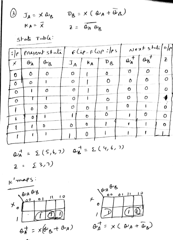
Add Answer to:
solve 1 2 and 3 Problems 1 and 2 require a 7-segment display. You may want to re-use the display driver you developed in Lab 3. Use a push-button as the clock - the pushbuttons are debounced, whereas...
6. Design a 2-bit binary counter that counts, 0, 1, 2, 3, 0,. Use the 74LS374 IC, which has eight D flip-flops on it. They are positive-edge triggered, but it will not matter at all here You may draw...
 6. Design a 2-bit binary counter that counts, 0, 1, 2, 3, 0,. Use the 74LS374 IC, which has eight D flip-flops on it. They are positive-edge triggered, but it will not matter at all here You may draw a state diagram and then fill in the table Present State Q(t) Next State (D(t) - Q(t+1)) Q1(t) Qo(t) 7. Design a BCD binary counter that counts from 0 to 9 then back to 0 and repeat, displaying the count on...
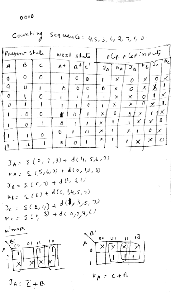
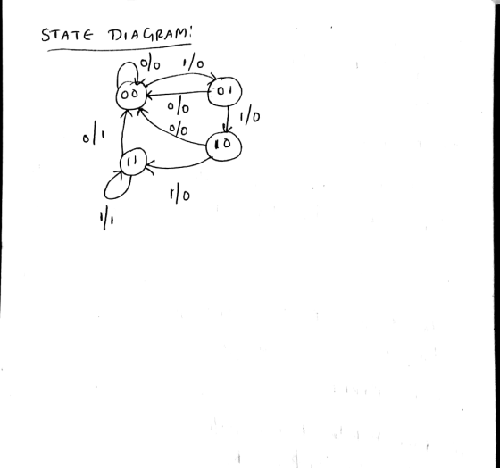
Design a 3-bit counter with counting sequence of 1, 3, 7, 2. Note: Use the symbol...
Design a 3-bit counter with counting sequence of 1, 3, 7, 2. Note: Use the symbol in order of CBA. (1) Draw the resulting circuit using JK-type flip flops. (2) Draw the complete state diagram corresponding to your circuit.
Consider the circuit in Figure 1. It is a 4-bit (QQ2Q3) synchronous counter which uses four T-typ...
 Consider the circuit in Figure 1. It is a 4-bit (QQ2Q3) synchronous counter which uses four T-type flip-flops. The counter increases its value on each positive edge of the clock if the Enable signal is asserted. The counter is reset to 0 by setting the Clear signal low. You are to implement an 8-bit counter of this type Enable T Q Clock Clear Figure 1. 4-bit synchronous counter (but you need to implement 8-bit counter in this lab) Specific notes:...
You will build a seven-segment display decoder, shown in Figure 3. The circuit has four input...
You will build a seven-segment display decoder, shown in Figure 3. The circuit has four input bits, D3:0 (representing a hexadecimal number between 0 and F), and produces seven output bits, Sa:g, that drive the seven segments to display the number. The 7-segment display we will use in this lab is a common cathode type, a segment of the display turns on when it is 1. The other type of 7-segment display is common anode, for which a segment turns...
hi i need answers for nos. 18-28. 1. In a counter, a flip-flop output 10. A...
 hi i need answers for nos. 18-28.
1. In a counter, a flip-flop output 10. A is a group of flip-flops, each one of which transition serves as a source for triggering other flip-flops, not by the common clock pulses. shares a common clock and is capable of storing one bit of information. A) RAM B) latch A ripple Cring (rather than signal transitions) are referred to as B synchronous D binary C) counter D) register 11. The Characteristic Equation...
hi i need answers for nos. 18-28.
1. In a counter, a flip-flop output 10. A is a group of flip-flops, each one of which transition serves as a source for triggering other flip-flops, not by the common clock pulses. shares a common clock and is capable of storing one bit of information. A) RAM B) latch A ripple Cring (rather than signal transitions) are referred to as B synchronous D binary C) counter D) register 11. The Characteristic Equation...
Objective: In this lab, we will learn how we can design sequential circuits using behavioral mode...
 Just need the code for the
random counter,Thanks
Objective: In this lab, we will learn how we can design sequential circuits using behavioral modelling, and implementing the design in FPGA. Problem: Design a random counter with the following counting sequence: Counting Sequence: 04 2 9 168573 Design Description: The counter has one clock (Clock), one reset (Reset), and one move left or right control signal (L/R) as input. The counter also has one 4bit output O and one 2bit output...
Just need the code for the
random counter,Thanks
Objective: In this lab, we will learn how we can design sequential circuits using behavioral modelling, and implementing the design in FPGA. Problem: Design a random counter with the following counting sequence: Counting Sequence: 04 2 9 168573 Design Description: The counter has one clock (Clock), one reset (Reset), and one move left or right control signal (L/R) as input. The counter also has one 4bit output O and one 2bit output...
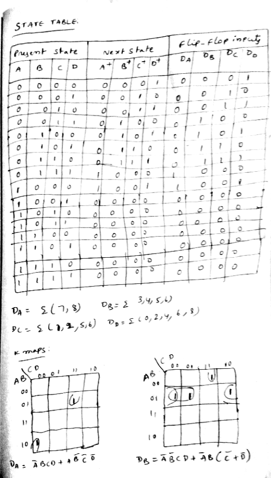
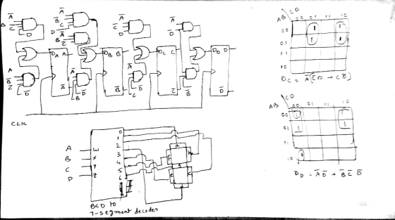
how slove 4-34, 4-35, 4-36??? I dont know that! please hlep me! 306 □ CHAPTER 4/SEQUENTIAL CIRCUITS OTABLE 4-16...
 how slove 4-34, 4-35, 4-36??? I dont know that! please hlep me!
306 □ CHAPTER 4/SEQUENTIAL CIRCUITS OTABLE 4-16 State Table for Problem 4-33 Next State Input Output Present State 4-36 4-37 0 0 0 0 4-38 Design the circuit specified by Table 4-14 and use the sequence from Problen 4-31 (either yours or the one posted on the text website) to perform an automatic logic simulation-based verification of your design. 4 433. The state table for a sequential circuit...
how slove 4-34, 4-35, 4-36??? I dont know that! please hlep me!
306 □ CHAPTER 4/SEQUENTIAL CIRCUITS OTABLE 4-16 State Table for Problem 4-33 Next State Input Output Present State 4-36 4-37 0 0 0 0 4-38 Design the circuit specified by Table 4-14 and use the sequence from Problen 4-31 (either yours or the one posted on the text website) to perform an automatic logic simulation-based verification of your design. 4 433. The state table for a sequential circuit...
In this lab, you will design a finite state machine to control the tail lights of...
 In this lab, you will design a finite state machine to control the tail lights of an unsual car. There are three lights on each side that operate in sequence to indicate thedirection of a turn. Figure ! shows the tail lights and Figure 2 shows the flashing sequence for (a) left turns and (b) right rums. ZOTTAS Figure 28:8: BCECECece BCECECECes BCECECECB BCECECBCB 8888 Figure 2 Part 1 - FSM Design Start with designing the state transition diagram for...
 6. Design a 2-bit binary counter that counts, 0, 1, 2, 3, 0,. Use the 74LS374 IC, which has eight D flip-flops on it. They are positive-edge triggered, but it will not matter at all here You may draw a state diagram and then fill in the table Present State Q(t) Next State (D(t) - Q(t+1)) Q1(t) Qo(t) 7. Design a BCD binary counter that counts from 0 to 9 then back to 0 and repeat, displaying the count on...
 Consider the circuit in Figure 1. It is a 4-bit (QQ2Q3) synchronous counter which uses four T-type flip-flops. The counter increases its value on each positive edge of the clock if the Enable signal is asserted. The counter is reset to 0 by setting the Clear signal low. You are to implement an 8-bit counter of this type Enable T Q Clock Clear Figure 1. 4-bit synchronous counter (but you need to implement 8-bit counter in this lab) Specific notes:...
 hi i need answers for nos. 18-28.
1. In a counter, a flip-flop output 10. A is a group of flip-flops, each one of which transition serves as a source for triggering other flip-flops, not by the common clock pulses. shares a common clock and is capable of storing one bit of information. A) RAM B) latch A ripple Cring (rather than signal transitions) are referred to as B synchronous D binary C) counter D) register 11. The Characteristic Equation...
hi i need answers for nos. 18-28.
1. In a counter, a flip-flop output 10. A is a group of flip-flops, each one of which transition serves as a source for triggering other flip-flops, not by the common clock pulses. shares a common clock and is capable of storing one bit of information. A) RAM B) latch A ripple Cring (rather than signal transitions) are referred to as B synchronous D binary C) counter D) register 11. The Characteristic Equation...
 Just need the code for the
random counter,Thanks
Objective: In this lab, we will learn how we can design sequential circuits using behavioral modelling, and implementing the design in FPGA. Problem: Design a random counter with the following counting sequence: Counting Sequence: 04 2 9 168573 Design Description: The counter has one clock (Clock), one reset (Reset), and one move left or right control signal (L/R) as input. The counter also has one 4bit output O and one 2bit output...
Just need the code for the
random counter,Thanks
Objective: In this lab, we will learn how we can design sequential circuits using behavioral modelling, and implementing the design in FPGA. Problem: Design a random counter with the following counting sequence: Counting Sequence: 04 2 9 168573 Design Description: The counter has one clock (Clock), one reset (Reset), and one move left or right control signal (L/R) as input. The counter also has one 4bit output O and one 2bit output...
 how slove 4-34, 4-35, 4-36??? I dont know that! please hlep me!
306 □ CHAPTER 4/SEQUENTIAL CIRCUITS OTABLE 4-16 State Table for Problem 4-33 Next State Input Output Present State 4-36 4-37 0 0 0 0 4-38 Design the circuit specified by Table 4-14 and use the sequence from Problen 4-31 (either yours or the one posted on the text website) to perform an automatic logic simulation-based verification of your design. 4 433. The state table for a sequential circuit...
how slove 4-34, 4-35, 4-36??? I dont know that! please hlep me!
306 □ CHAPTER 4/SEQUENTIAL CIRCUITS OTABLE 4-16 State Table for Problem 4-33 Next State Input Output Present State 4-36 4-37 0 0 0 0 4-38 Design the circuit specified by Table 4-14 and use the sequence from Problen 4-31 (either yours or the one posted on the text website) to perform an automatic logic simulation-based verification of your design. 4 433. The state table for a sequential circuit...
 In this lab, you will design a finite state machine to control the tail lights of an unsual car. There are three lights on each side that operate in sequence to indicate thedirection of a turn. Figure ! shows the tail lights and Figure 2 shows the flashing sequence for (a) left turns and (b) right rums. ZOTTAS Figure 28:8: BCECECece BCECECECes BCECECECB BCECECBCB 8888 Figure 2 Part 1 - FSM Design Start with designing the state transition diagram for...
Most questions answered within 3 hours.
-
4. Without doing any calculations, predict whether the observed
∆T would increase, decrease or remain the...
asked 53 minutes ago -
Based on the range, which of the following sets of scores has
the greatest variability? 3,...
asked 2 hours ago -
Ripples in a pond travel at a velocity of 3 m/s with one peak
passing a...
asked 1 hour ago -
A man stands on the roof of a building of height 13.0 mm and
throws a...
asked 1 hour ago -
The extent to which assets are financed by borrowed funds and
other liabilities is indicated by:...
asked 2 hours ago -
Explain in detail
Germany is the fifth largest economy
explain what goods and services Germany specializes...
asked 3 hours ago -
The density of platinum is 21.45 g/mL. If a cube of platinum
with a mass of...
asked 3 hours ago -
Accounts Receivable
Sales
A/R Posting
Extended Sales Invoice
Packing Slip
Compare invoice to packing slip 2...
asked 3 hours ago -
Michaella, age 23, is a full-time law student and is claimed by
her parents as a...
asked 3 hours ago -
Why are polymers not typically casted into products?
asked 3 hours ago -
When rolling a die 129 times, what is the probability of rolling
a 6 no more...
asked 3 hours ago -
4. A call option currently sells for $7.75. It has a strike
price of $85 and...
asked 3 hours ago