
Homework Answers

Add Answer to:
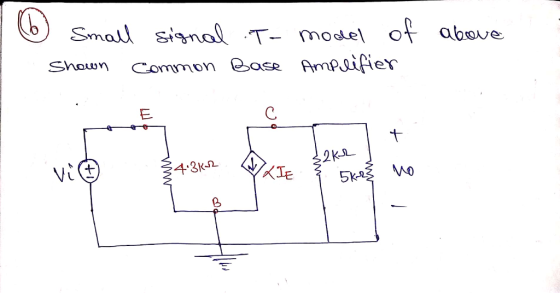
An npn transistor is employed in a common-base amplifier. 4 p 100, VBE 0.7 V. +-5V 2Ks2 Vo 5ΚΩ 4.3KM -5V in It is known that the device is biased to have Ig of 1 mA. Determine the transconductance of...
In the amplifier circuit below, the transistor has the following properties:Vt =1.5V,k’n=100 microA/V2,W=2 micro m ,L=0.2...
 In the amplifier circuit below, the transistor has the following
properties:Vt =1.5V,k’n=100 microA/V2,W=2 micro m ,L=0.2 micro m,
lambda = 0V^-1
a. Find the dc values VG, VD, and VS.
b. Verify (prove) that the circuit is in the proper region of
operation for an amplifier
c. Find the transconductance value, gm
d. Draw the equivalent small-signal circuit model, replacing the
NMOS with its pi-model
e. Draw the equivalent small-signal circuit model, replacing the
NMOS with its T-model
f. Calculate...
In the amplifier circuit below, the transistor has the following
properties:Vt =1.5V,k’n=100 microA/V2,W=2 micro m ,L=0.2 micro m,
lambda = 0V^-1
a. Find the dc values VG, VD, and VS.
b. Verify (prove) that the circuit is in the proper region of
operation for an amplifier
c. Find the transconductance value, gm
d. Draw the equivalent small-signal circuit model, replacing the
NMOS with its pi-model
e. Draw the equivalent small-signal circuit model, replacing the
NMOS with its T-model
f. Calculate...
QUESTION (1) Transistor Mi in this common base amplifier circuit has the following characteristics: +Vc VTH...
 QUESTION (1) Transistor Mi in this common base amplifier circuit has the following characteristics: +Vc VTH =1 V Rp R, C. K 1 mA/V2 2 0.1 R Given: Vcc 2 mA, 10 V, lbias Ct C2 0, 5 k2, RD 2 k2 RI 10 k, R2 R (12 points) a) Determine the small signal gain, vo/Vin. (4 points) b) Determine the input resistance, Rin. (4 points) c) Determine the output resistance, Ro. Useful formulae: for n-channel MOSFET triode region =...
Ci-00 o Vo Qi RL-10k2 6 5 V Figure 2. I-500 μΑ, ka'(W/L)-1 mA/V2, IVI î.5V,...
 Ci-00 o Vo Qi RL-10k2 6 5 V Figure 2. I-500 μΑ, ka'(W/L)-1 mA/V2, IVI î.5V, VA-75V For the circuit shown in Figure 2: a) Find VD, Va, and Vas b) Draw a small signal equivalent circuit and find the model parameter values. c) Find the input and output resistances of the circuit. d) Find the open circuit voltage gain for the amplifier and the loaded voltage gain.
The 1 mA. V, ls -VE -15 15 V, in the following differential amplifier circuit, Vcc parameters are given as β, 100, VBE# 0.7 V, pr-25 mV, K.-100 V. transistor Rc-10 kΩ For: RE-150 Ω Rc Rc REE-200...
 The 1 mA. V, ls -VE -15 15 V, in the following differential amplifier circuit, Vcc parameters are given as β, 100, VBE# 0.7 V, pr-25 mV, K.-100 V. transistor Rc-10 kΩ For: RE-150 Ω Rc Rc REE-200 kΩ a) What is the input differential resistance, Rid b) What is the overall voltage gain vV? You c) What is input common mode resistance, d) What is the worst case common mode gain that appear across the two input terminals? (4...
#4 The accompanying circuit shows a 4-resistor biased JFET transistor Determine the values of Rp and Rs so that the Q-point is equal to, VDsq 10 V and IDg 5 mA . For the JFET take IDss = 10 mA...
 #4
The accompanying circuit shows a 4-resistor biased JFET transistor Determine the values of Rp and Rs so that the Q-point is equal to, VDsq 10 V and IDg 5 mA . For the JFET take IDss = 10 mA, VP =-5 V and λ 0 . The circuit parameters are, R1-740 k, R2-22 1.85 ka, Rs-85 ㏀ and RL-3.5 ㏀. Take the power supply VDD 24 V 2- Vo R1 Vi R2 Signal generator 4-In reference to the circuit...
#4
The accompanying circuit shows a 4-resistor biased JFET transistor Determine the values of Rp and Rs so that the Q-point is equal to, VDsq 10 V and IDg 5 mA . For the JFET take IDss = 10 mA, VP =-5 V and λ 0 . The circuit parameters are, R1-740 k, R2-22 1.85 ka, Rs-85 ㏀ and RL-3.5 ㏀. Take the power supply VDD 24 V 2- Vo R1 Vi R2 Signal generator 4-In reference to the circuit...
A common source amplifier circuit based on a single n-channel MOSFET is shown in Figure 4b. Assume that the transconductance gm-60 mS (equivalent to mA/ V) and drain source resistance, os,...
 A common source amplifier circuit based on a single n-channel MOSFET is shown in Figure 4b. Assume that the transconductance gm-60 mS (equivalent to mA/ V) and drain source resistance, os, is so large it may be neglected. 0) Calculate the open circuit voltage gain Av Yout/ Vis. i) The amplifier has a load of 10 k2. Determine the current gain Va. = 12 V 150k 4k3 Vout Vin 200k GND = 0 V Figure 4b a) State the name...
1. Design the common source amplifier shown in Figure 1 with Ip- 1 mA and Vo 5 V Determine V2 and Ri. The MOSFET characteristics are V-50 V, k-0.093 A/V, gate-to- drain capacitance, Cd 40 pF,...
 1. Design the common source amplifier shown in Figure 1 with Ip- 1 mA and Vo 5 V Determine V2 and Ri. The MOSFET characteristics are V-50 V, k-0.093 A/V, gate-to- drain capacitance, Cd 40 pF, and Vi 1.1 V. (For PSpice simulations, use parameters: VTO. 1.1 LAMBDA-002 KP-0.093 CGDO-4E-7 w=100u L-I00u for the 2N7000 MOSFET.) a. Determine the gain and gm of the circuit b. Determine the low-frequency (high-pass response) poles of the common-source amplifier due to the coupling...
4. Lab VIII: Experiment VII The Bipolar Junction Transistor (BJT) Characteristics The bipolar junction transistor (BJT)...
 4. Lab VIII: Experiment VII The Bipolar Junction Transistor (BJT) Characteristics The bipolar junction transistor (BJT) is a three-terminal solid state device widely used as an amplifier (or switching) device. It consists of two n-type materials sandwiched by p-type material (npn) or two p-type and n-type. The terminals (sections) are known as emitter E, base B and collector C. Two currents and two voltages uniquely describe the behavior of the device. The third current/voltage can be determined through KCL/KVL. See...
Electronics-common emmitter amplifier. Pls be try to be helpful Im trying to study here in this book example.. However im kinda lost and i cant follow the correct answers they got.. could someon...
 Electronics-common emmitter amplifier. Pls be try to be
helpful
Im trying to study here in this book example..
However im kinda lost and i cant follow the correct answers
they got.. could someone pls help me..
I just wanna learn this, i hope u can help me learn by showin
clear and corect solutions on how to properly got the
answer..
Also especially on finding the values on the laod line
analysis, im lost.
Pls help
Any helpful help would...
Electronics-common emmitter amplifier. Pls be try to be
helpful
Im trying to study here in this book example..
However im kinda lost and i cant follow the correct answers
they got.. could someone pls help me..
I just wanna learn this, i hope u can help me learn by showin
clear and corect solutions on how to properly got the
answer..
Also especially on finding the values on the laod line
analysis, im lost.
Pls help
Any helpful help would...
Problem 3: Design Problem On Figure P3a, you have a Common Source (CS) n-channel MOSFET amplifier....
 Problem 3: Design Problem On Figure P3a, you have a Common Source (CS) n-channel MOSFET amplifier. Notice the absence of a source resistor Rsig and load resistor R. If we know how the present amplifier (the one on Figure P3a) behaves without Rsig and RL, we can infer its behaviors if Rsig and R were to be added. design the amplifier circuit on Figure P3a, i.e., you have to find appropriate values for RGj You are to RG,, RD, and...
 In the amplifier circuit below, the transistor has the following
properties:Vt =1.5V,k’n=100 microA/V2,W=2 micro m ,L=0.2 micro m,
lambda = 0V^-1
a. Find the dc values VG, VD, and VS.
b. Verify (prove) that the circuit is in the proper region of
operation for an amplifier
c. Find the transconductance value, gm
d. Draw the equivalent small-signal circuit model, replacing the
NMOS with its pi-model
e. Draw the equivalent small-signal circuit model, replacing the
NMOS with its T-model
f. Calculate...
In the amplifier circuit below, the transistor has the following
properties:Vt =1.5V,k’n=100 microA/V2,W=2 micro m ,L=0.2 micro m,
lambda = 0V^-1
a. Find the dc values VG, VD, and VS.
b. Verify (prove) that the circuit is in the proper region of
operation for an amplifier
c. Find the transconductance value, gm
d. Draw the equivalent small-signal circuit model, replacing the
NMOS with its pi-model
e. Draw the equivalent small-signal circuit model, replacing the
NMOS with its T-model
f. Calculate...
 QUESTION (1) Transistor Mi in this common base amplifier circuit has the following characteristics: +Vc VTH =1 V Rp R, C. K 1 mA/V2 2 0.1 R Given: Vcc 2 mA, 10 V, lbias Ct C2 0, 5 k2, RD 2 k2 RI 10 k, R2 R (12 points) a) Determine the small signal gain, vo/Vin. (4 points) b) Determine the input resistance, Rin. (4 points) c) Determine the output resistance, Ro. Useful formulae: for n-channel MOSFET triode region =...
 Ci-00 o Vo Qi RL-10k2 6 5 V Figure 2. I-500 μΑ, ka'(W/L)-1 mA/V2, IVI î.5V, VA-75V For the circuit shown in Figure 2: a) Find VD, Va, and Vas b) Draw a small signal equivalent circuit and find the model parameter values. c) Find the input and output resistances of the circuit. d) Find the open circuit voltage gain for the amplifier and the loaded voltage gain.
 The 1 mA. V, ls -VE -15 15 V, in the following differential amplifier circuit, Vcc parameters are given as β, 100, VBE# 0.7 V, pr-25 mV, K.-100 V. transistor Rc-10 kΩ For: RE-150 Ω Rc Rc REE-200 kΩ a) What is the input differential resistance, Rid b) What is the overall voltage gain vV? You c) What is input common mode resistance, d) What is the worst case common mode gain that appear across the two input terminals? (4...
 #4
The accompanying circuit shows a 4-resistor biased JFET transistor Determine the values of Rp and Rs so that the Q-point is equal to, VDsq 10 V and IDg 5 mA . For the JFET take IDss = 10 mA, VP =-5 V and λ 0 . The circuit parameters are, R1-740 k, R2-22 1.85 ka, Rs-85 ㏀ and RL-3.5 ㏀. Take the power supply VDD 24 V 2- Vo R1 Vi R2 Signal generator 4-In reference to the circuit...
#4
The accompanying circuit shows a 4-resistor biased JFET transistor Determine the values of Rp and Rs so that the Q-point is equal to, VDsq 10 V and IDg 5 mA . For the JFET take IDss = 10 mA, VP =-5 V and λ 0 . The circuit parameters are, R1-740 k, R2-22 1.85 ka, Rs-85 ㏀ and RL-3.5 ㏀. Take the power supply VDD 24 V 2- Vo R1 Vi R2 Signal generator 4-In reference to the circuit...
 A common source amplifier circuit based on a single n-channel MOSFET is shown in Figure 4b. Assume that the transconductance gm-60 mS (equivalent to mA/ V) and drain source resistance, os, is so large it may be neglected. 0) Calculate the open circuit voltage gain Av Yout/ Vis. i) The amplifier has a load of 10 k2. Determine the current gain Va. = 12 V 150k 4k3 Vout Vin 200k GND = 0 V Figure 4b a) State the name...
 1. Design the common source amplifier shown in Figure 1 with Ip- 1 mA and Vo 5 V Determine V2 and Ri. The MOSFET characteristics are V-50 V, k-0.093 A/V, gate-to- drain capacitance, Cd 40 pF, and Vi 1.1 V. (For PSpice simulations, use parameters: VTO. 1.1 LAMBDA-002 KP-0.093 CGDO-4E-7 w=100u L-I00u for the 2N7000 MOSFET.) a. Determine the gain and gm of the circuit b. Determine the low-frequency (high-pass response) poles of the common-source amplifier due to the coupling...
 4. Lab VIII: Experiment VII The Bipolar Junction Transistor (BJT) Characteristics The bipolar junction transistor (BJT) is a three-terminal solid state device widely used as an amplifier (or switching) device. It consists of two n-type materials sandwiched by p-type material (npn) or two p-type and n-type. The terminals (sections) are known as emitter E, base B and collector C. Two currents and two voltages uniquely describe the behavior of the device. The third current/voltage can be determined through KCL/KVL. See...
 Electronics-common emmitter amplifier. Pls be try to be
helpful
Im trying to study here in this book example..
However im kinda lost and i cant follow the correct answers
they got.. could someone pls help me..
I just wanna learn this, i hope u can help me learn by showin
clear and corect solutions on how to properly got the
answer..
Also especially on finding the values on the laod line
analysis, im lost.
Pls help
Any helpful help would...
Electronics-common emmitter amplifier. Pls be try to be
helpful
Im trying to study here in this book example..
However im kinda lost and i cant follow the correct answers
they got.. could someone pls help me..
I just wanna learn this, i hope u can help me learn by showin
clear and corect solutions on how to properly got the
answer..
Also especially on finding the values on the laod line
analysis, im lost.
Pls help
Any helpful help would...
 Problem 3: Design Problem On Figure P3a, you have a Common Source (CS) n-channel MOSFET amplifier. Notice the absence of a source resistor Rsig and load resistor R. If we know how the present amplifier (the one on Figure P3a) behaves without Rsig and RL, we can infer its behaviors if Rsig and R were to be added. design the amplifier circuit on Figure P3a, i.e., you have to find appropriate values for RGj You are to RG,, RD, and...
Most questions answered within 3 hours.
-
A company project has an initial cost of $40,000, expected net
cash flows of $9,000 per...
asked 6 seconds ago -
How do you use strategy in your current position or how does
your current position align...
asked 2 minutes ago -
a person's ability to be properly diagnosed with a
disease/condition can be affected by the person;s...
asked 1 minute ago -
John needs 40 Eternal Light flashlights. Each Eternal Light
flashlight requires 3 bulbs, and each bulb...
asked 9 minutes ago -
1) If Nominal GDP is $16,000 billion and the GDP deflator is 50,
then Real GDP...
asked 15 minutes ago -
D. A student completed 20 courses in the School of Arts and
Sciences. Her grades in...
asked 1 hour ago -
teo
pucks moving on a frictionless air table are about to collide. the
1.5 kg puck...
asked 2 hours ago -
Problem #1
The area between Z = 0 and Z = 2.50
The area between Z...
asked 3 hours ago -
1. What is the meaning of the term communication style?
2. What are the benefits to...
asked 3 hours ago -
9.) You are buying a car that cost $26,500. You make payments of
$412 each month...
asked 3 hours ago -
. Suppose a discrete random variable has probability
distribution
P(x) = .2 if x = 0...
asked 4 hours ago -
Under the influence of its drive force, a snowmobile is moving
at a constant velocity along...
asked 5 hours ago